Optical switch

a technology of optical switches and switches, applied in the field of optical switches, can solve the problems of high power consumption of optical switches, slow switching speed (several seconds or more), propagation loss, etc., and achieve the effect of low power consumption and higher speed

Inactive Publication Date: 2006-06-29
KEIO UNIV
View PDF4 Cites 33 Cited by
  • Summary
  • Abstract
  • Description
  • Claims
  • Application Information

AI Technical Summary

Benefits of technology

[0024] Effects obtained out of representative examples of the present invention are briefly described as follows.
[0025] Since the optical switch uses a phase change material with memory feature, an optical switch that is capable of a self-holding operation without the necessity for maintaining a power distribution and a light irradiation and is low in power consumption can be constructed. By utilizing the memory feature, optical information can be recorded corresponding to a switch state, which makes it possible to read out recorded optical information according to an output position of a reading light. An optical memory of an all-optical type that performs input/output and control by use of light can be constructed, which makes it possible to simultaneously realize a variable delay function (function to vary delay time necessary for passing through the present optical switch), a time switch function (function to switch timeslots of light pulses that carry information), and a wavelength conversion function (function to differentiate an output light wavelength from an input light wavelength).
[0026] In addition, the phase change material such as chalcogenide changes from crystal to an amorphous state in less than a nanosecond, and a change f...

Problems solved by technology

However, since these optical switches have no self-holding function, it is necessary to supply current at all times or to apply voltage at all times so as to maintain switch states.
Therefore, these optical switches have a drawback in high power consumption.
However, there is a drawback in that the switching speed is slow (several seconds or more) since a change in molecular orientation is involved and in that light having two different wavelengths is necessary for switching.
Therefore, a propagation loss owing to a convergence of a propagation light into the...

Method used


Image

  • Optical switch
  • Optical switch
  • Optical switch

Examples


embodiment 1

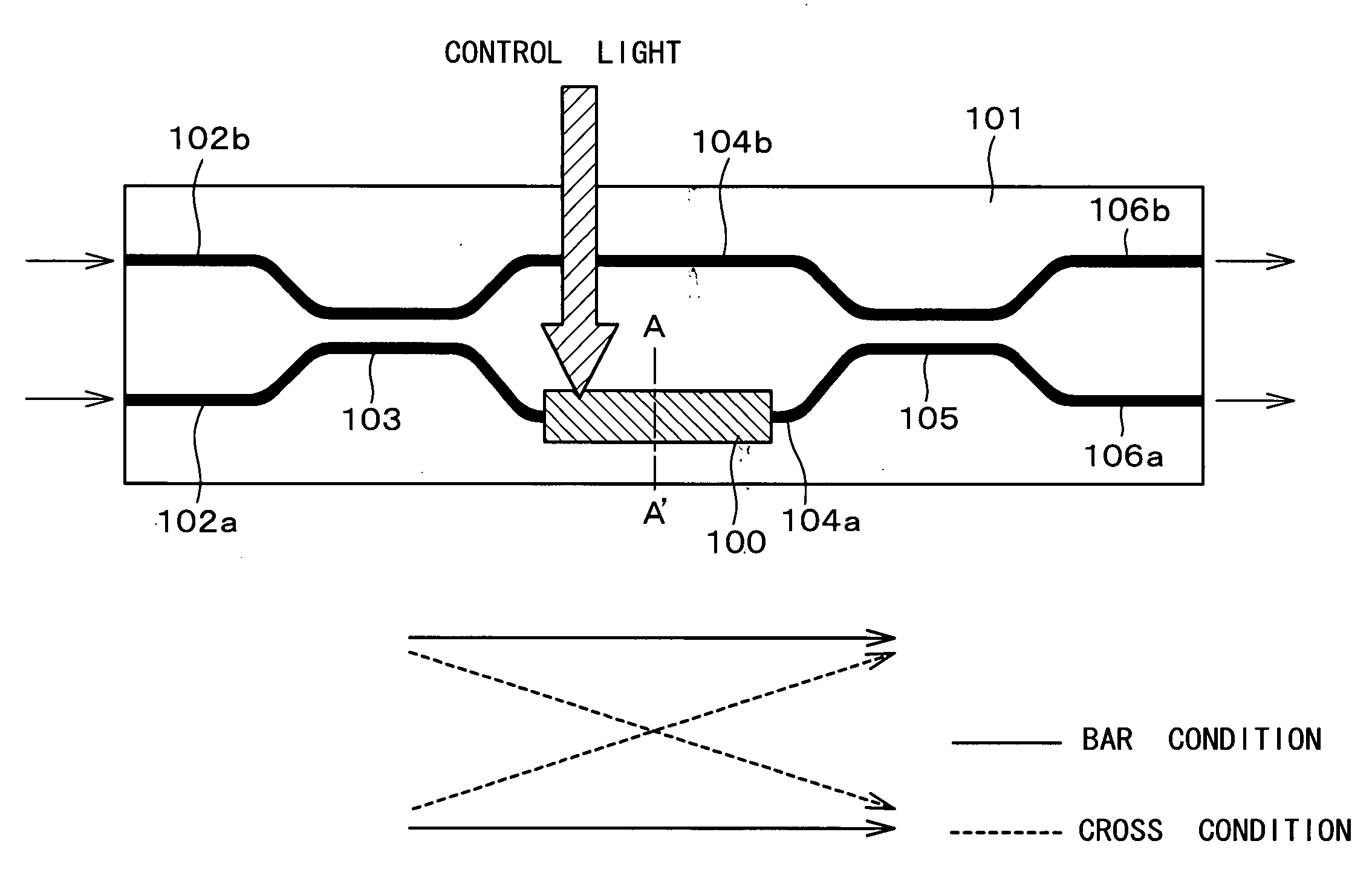
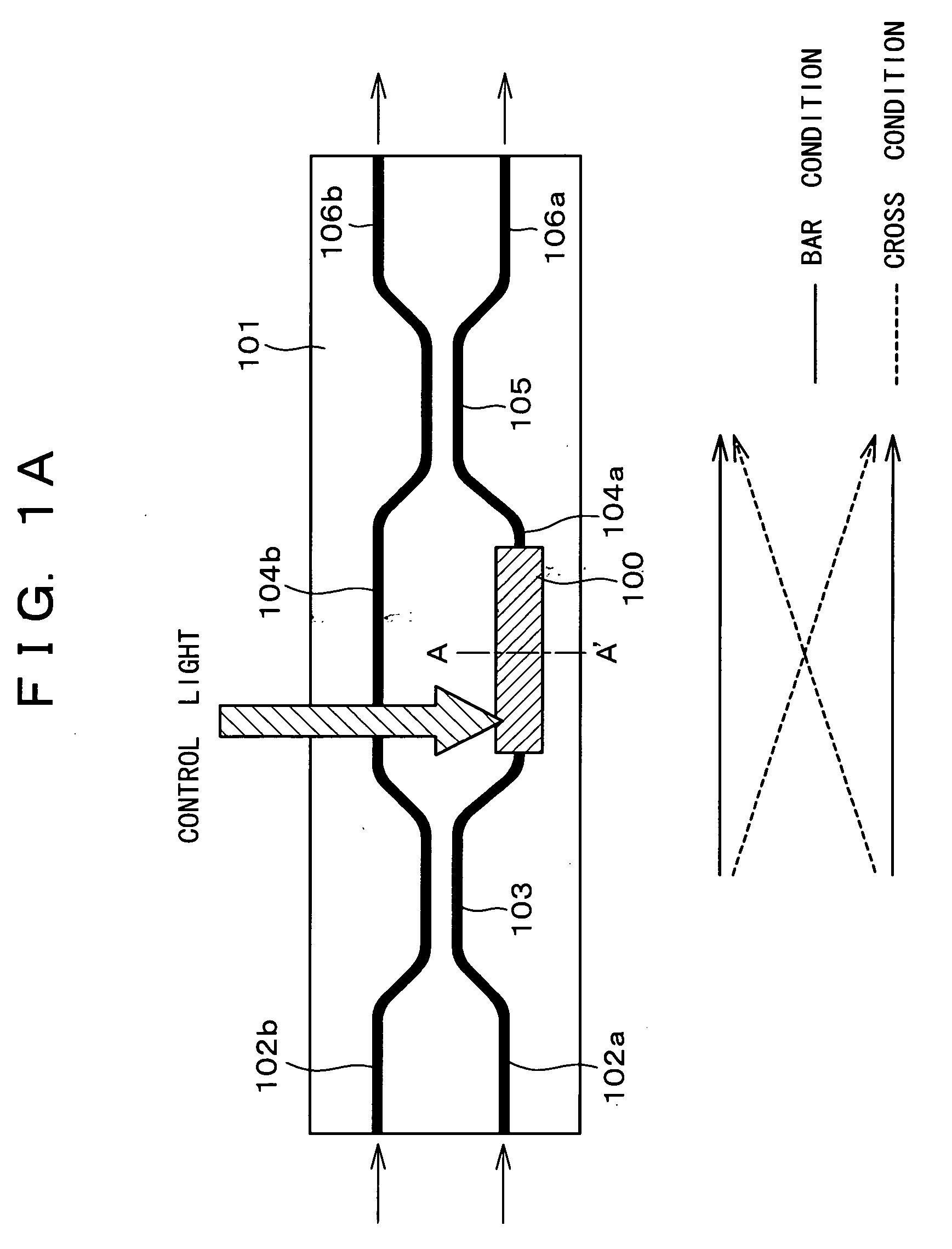
[0057]FIG. 1A to FIG. 1J are views showing configurations of an optical switch according to Embodiment 1 of the present invention. FIG. 1A is a top view thereof. The optical switch of Embodiment 1 is composed of a quartz substrate 101, first and second input waveguides 102a and 102b, a first directional coupler 103, first and second arm waveguides 104a and 104b of a Mach-Zehnder interferometric circuit, a second directional coupler 105, first and second output waveguides 106a and 106b, and a phase change material portion 100 as a region. Details of this phase change material portion 100 as a region are shown in the following.

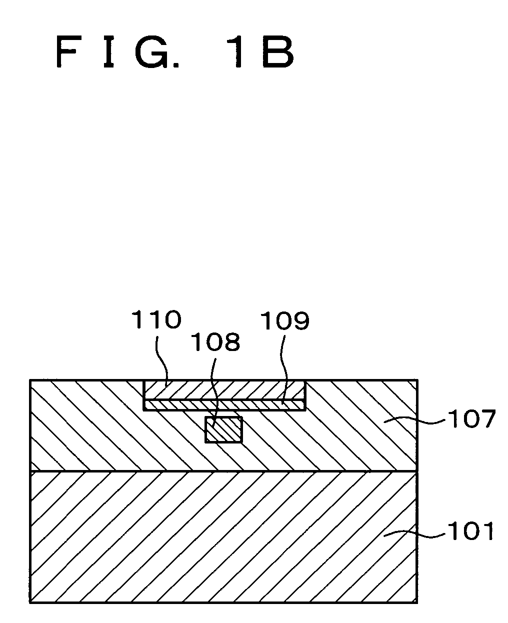
[0058]FIG. 1B is a sectional view along A-A′ of FIG. 1A. An optical switch according to Embodiment 1 in this section is composed of a quartz substrate 101, a cladding 107, a core 108, a phase change material portion 109, and a sealing resin 110. The sealing resin 110 has a refractive index equivalent to that of the cladding 107, seals the phase change material ...

embodiment 2

[0070]FIG. 2A to FIG. 2D are top views showing configurations of an optical switch according to Embodiment 2 of the present invention.

[0071]FIG. 2A shows a configuration where phase change material portions are symmetrically arranged on two arm waveguides. Since this is a symmetrical structure, it is easy to equalize the respective arm waveguides in propagation loss, which makes it possible to raise the extinction ratio of the optical switch. In addition, it is also possible to irradiate light onto both arm waveguides so as to cause a push-pull operation by changing one from an amorphous state to a crystal state and the other from a crystal state to an amorphous state.

[0072]FIG. 2B is a configuration where phase change material portions are provided at an optical coupling part of a directional coupler. Although fabrication accuracy is required, this is suitable for a reduction in size.

[0073]FIG. 2C is a configuration where phase change material portions are provided at parts of a...

embodiment 3

[0075]FIG. 3 is a sectional view showing a configuration of an optical switch according to Embodiment 3 of the present invention. In the optical switch of Embodiment 3, a phase change material portion 109 is processed into thin lines having roughly a 10 nm to 200 nm width or island-shaped grains having a diameter of 10 nm to 200 nm. Phase change characteristics of the phase change material portion 109 greatly change depending on its grain diameter. By such a miniaturization, phase transition time can be reduced to construct a high-speed switch.


PUM


Abstract

In order to provide a low-loss optical switch that is low in power consumption by providing the same as a self-holding type, and high speed and highly practicable, an optical switch of the present invention is composed of a quartz substrate (101), first and second input waveguides (102a and 102b), a first directional coupler (103), first and second arm waveguides (104a and 104b) of a Mach-Zehnder interferometric circuit, a second directional coupler (105), first and second output waveguides (106a and 106b), and a phase change material portion (100). A control light (for an amorphous to crystal transition) pulse (pulse width: 20 ns, pulse intensity: 5 mW) having a wavelength of 0.78 microns is irradiated. As a result of the control light pulse irradiation, the phase change material portion (109) changes in phase to a crystal state, and the optical switch transits to a bar condition.

Description

BACKGROUND OF THE INVENTION [0001] 1. Field of the Invention [0002] The present invention relates to an optical switch that is effective for application to a switching process circuit of an optical communications network node. [0003] 2. Description of the Related Art [0004]FIG. 10a is a view showing a configuration and operation mechanism of a conventional optical switch. This conventional optical switch is composed of input waveguides 102, a 2×2 first directional coupler 103, two single-mode waveguides 104, a 2×2 second directional coupler 105, and output waveguides 106. The material is quartz. One of the two single-mode waveguides 104 is provided with a heater electrode 150 for controlling temperature. When an electric current is supplied to the heater electrode 150 to change the temperature, the refractive index of the single-mode waveguide 104b in the vicinity of the heater electrode 150 is changed. Therefore, a phase difference in light waves occurs between the single-mode wave...

Claims


Application Information

Patent Timeline
IPC IPC(8): G02B6/26
CPCG02B6/12004G02B6/12007G02B6/124G02F1/0338G02F1/293G02F1/3136G02F2202/13
Inventor TSUDA, HIROYUKISAIKI, TOSHIHARU
Owner KEIO UNIV
Why Eureka
Try Eureka