
Chemically amplified positive photoresist composition for thick film, thick-film photoresist laminated product, manufacturing method for thick-film resist pattern, and manufacturing method for connection terminal

Active Publication Date: 2006-06-29
TOKYO OHKA KOGYO CO LTD
View PDF2 Cites 26 Cited by
  • Summary
  • Abstract
  • Description
  • Claims
  • Application Information

AI Technical Summary

Benefits of technology

[0021] The present invention takes the above problems associated with the conventional technology into consideration, with an object of providing a chemically amplified positive photoresist composition for thick film, which enables the formation of a plated product with a favorable shape, displays excellent stress resistance, plating solution resistance, and plating resistance, offers high sensitivity, and is ideal for manufacturing connection terminals and the like, as well as providing a thick-film photoresist laminated product, a manufacturing method for a thick-film resist pattern that uses the laminated product, and a manufacturing method for a connection terminal.
[0039] The present invention provides a chemically amplified positive photoresist composition for thick film, which enables the formation of a plated product with a favorable shape, displays excellent plating resistance and a high level of contrast, and is ideal for manufacturing connection terminals and the like, as well as providing a thick-film photoresist laminated product, a manufacturing method for a thick-film resist pattern that uses the laminated product, and a manufacturing method for a connection terminal.
[0040] Using a chemically amplified positive photoresist composition for thick film of the first aspect of the present invention enables particularly favorable formation of resist patterns with aspect ratios of 2 or greater, and this enables the formation of resist-free patterns (resist-free portions) with aspect ratios of 2 or greater. Using a chemically amplified positive photoresist composition for thick film according to the first aspect of the present invention even enables the formation of resist patterns with an aspect ratio of 10, and resist-free patterns (resist-free portions) based on such resist patterns.

Problems solved by technology

However, when the conventional types of chemically amplified photoresist compositions disclosed in the patent references 2 and 3 are used to produce a thick-film resist layer, because the stress resistance of the photoresist composition to plating is unsatisfactory, the metal layer obtained from the plating treatment tends to swell, making it difficult to achieve a favorable pattern for the plated product.
Furthermore, the resistance of the photoresist composition to the plating solution is also inadequate, with chips and cracks developing in the resist either during the plating step or during the washing step following plating, making conducting multiple plating steps with the same resist pattern essentially impossible (poor plating resistance).
Furthermore, with the photosensitive resin composition comprising a compound containing a naphthoquinone diazide group disclosed in the patent reference 1, which displays superior plating resistance, improving the sensitivity is problematic.

Method used


Image

  • Chemically amplified positive photoresist composition for thick film, thick-film photoresist laminated product, manufacturing method for thick-film resist pattern, and manufacturing method for connection terminal
  • Chemically amplified positive photoresist composition for thick film, thick-film photoresist laminated product, manufacturing method for thick-film resist pattern, and manufacturing method for connection terminal
  • Chemically amplified positive photoresist composition for thick film, thick-film photoresist laminated product, manufacturing method for thick-film resist pattern, and manufacturing method for connection terminal

Examples


synthesis example 1

[0121] A flask equipped with a stirrer, a reflux condenser, a thermometer, and a dropping funnel was flushed with nitrogen, and subsequently charged with propylene glycol methyl ether acetate as a solvent, and stirring of the solvent was then initiated. The temperature of the solvent was then raised to 80° C. The dropping funnel was charged with 2,2′-azobisisobutyronitrile as a polymerization catalyst, 50% by weight of 1-ethylcyclohexyl methacrylate as the unit (b1), and 50% by weight of 2-ethoxyethyl acrylate as the structural unit (b2), and following stirring to dissolve the polymerization catalyst, the resulting solution was added dropwise to the flask at a uniform rate over 3 hours. Reaction was then continued for a further 5 hours at 80° C. to allow the polymerization to proceed. The temperature was then cooled to room temperature, yielding a resin of the component (B).

[0122] This resin was then fractionated, yielding 5 resins (B-1) to (B-5) with the different weight average m...

synthesis example 2

[0128] With the exceptions of using 20% by weight of 1-ethylcyclohexyl methacrylate as the structural unit (b1), and 80% by weight of 2-ethoxyethyl acrylate as the structural unit (b2), reaction was conducted in the same manner as the synthesis example 1, yielding a resin (B-6) with a weight average molecular weight of 350,000.

synthesis example 3

[0129] With the exceptions of using 80% by weight of 1-ethylcyclohexyl methacrylate as the structural unit (b1), and 20% by weight of 2-ethoxyethyl acrylate as the structural unit (b2), reaction was conducted in the same manner as the synthesis example 1, yielding a resin (B-7) with a weight average molecular weight of 350,000.


PUM

PropertyMeasurementUnit
Lengthaaaaaaaaaa
Thicknessaaaaaaaaaa
Thicknessaaaaaaaaaa

Abstract

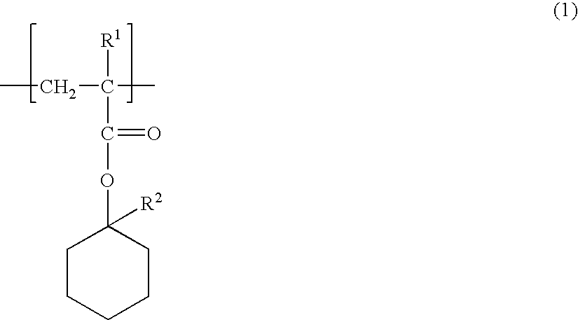
A chemically amplified positive photoresist composition for thick film that is used for forming a thick-film photoresist layer with a film thickness of 10 to 150 μm on top of a support, including (A) a compound that generates acid on irradiation with active light or radiation, and (B) a resin that displays increased alkali solubility under the action of acid, wherein the component (B) includes a resin formed from a copolymer containing a structural unit (b1) with a specific structure.

Description

BACKGROUND OF THE INVENTION [0001] 1. Field of the Invention [0002] The present invention relates to a chemically amplified positive photoresist composition for thick film, a thick-film photoresist laminated product, a manufacturing method for a thick-film resist pattern, and a manufacturing method for a connection terminal. More specifically, the present invention relates to a chemically amplified positive photoresist composition for thick film, a thick-film photoresist laminated product, a manufacturing method for a thick-film resist pattern, and a manufacturing method for a connection terminal, which are ideal for use in the formation of connection terminals such as bumps or metal posts, and wiring patterns, during both the manufacture of circuit substrates, and the manufacture of electronic components such as CSP (chip size packages) that are mounted on such circuit substrates. [0003] 2. Description of Related Art [0004] Photofabrication, which is now the most widely used techni...

Claims


Application Information

Patent Timeline
IPC IPC(8): G03C1/76
CPCG03F7/0397Y10S430/111
Inventor OKUI, TOSHIKIMISUMI, KOICHI
Owner TOKYO OHKA KOGYO CO LTD
Learn More