Wire bonds having pressure-absorbing balls

a technology of pressure-absorbing balls and wire bonds, which is applied in the direction of non-electric welding apparatus, manufacturing tools, and soldering equipment, etc., can solve the problems of reducing the risk of cracking damage, and reducing the size of the dielectric pattern

Active Publication Date: 2006-07-06
TEXAS INSTR INC
View PDF15 Cites 5 Cited by
  • Summary
  • Abstract
  • Description
  • Claims
  • Application Information

AI Technical Summary

Benefits of technology

[0011] It is a technical advantage of the invention to eliminate restrictions on the size of the dielectric pattern, thus minimizing the risks of inflicting cracking damage even to very brittle dielectrics.
[0012] It is another technical advantage of the invention to provide design concepts and process methods which are flexible so that they can be applied to several families of products, and are general, so that they can be applied to several generations of products. The invention supports the ongoing miniaturization trend in the semiconductor industry, especially the shrinking of bond pad diameters.
[0013] Another object of the invention is to use only processes already employed in the fabrication of integrated circuit devices, thus avoiding the cost of new capital investment and using the installed fabrication equipment base.
[0014] The technical advances represented by certain embodiments of the invention will become apparent from the following description of the preferred embodiments of the invention, when considered in conjunction with the accompanying drawings and the novel features set forth in the appended claims.

Problems solved by technology

It is well known in semiconductor technology that bond pads on silicon integrated circuits can be damaged during conventional thermosonic wire bonding to circuit bond pad made of aluminum or copper.
Mechanical loading and ultrasonic stresses applied by the tip of the bonding capillary to the bond pad are particularly suspect.
When the damage is not apparent during the bonding process, the defects may manifest themselves subsequently by succumbing to thermo-mechanical stresses generated during plastic encapsulation, accelerated reliability testing, temperature cycling, and device operation.
The damage appears in most cases as microcracks which may progress to fatal fractures in the underlying dielectric, as chip-outs of brittle or mechanically weak dielectric films, often together with pieces of metal or silicon, or as lifted ball bonds or delamination of metal layers.
Since these materials are also used under the bond pad metal, they magnify the risk of device failure by cracking.
Again, the risk of yield loss and lowered reliability is enhanced.
Attempts to solve these problems by using softer wires and attachments balls have failed because these wires sag under their own weight in long-looping spans, or can be swept in the transfer molding process.
In addition, these difficulties tend to get aggravated, when larger wire diameters are needed to keep the electrical resistance of long loops at an acceptable value.
Furthermore, bonding balls made from these large-diameter wires would end up with ball diameters too large for the ever shrinking pad sizes.

Method used


Image

  • Wire bonds having pressure-absorbing balls
  • Wire bonds having pressure-absorbing balls
  • Wire bonds having pressure-absorbing balls

Examples


Embodiment Construction

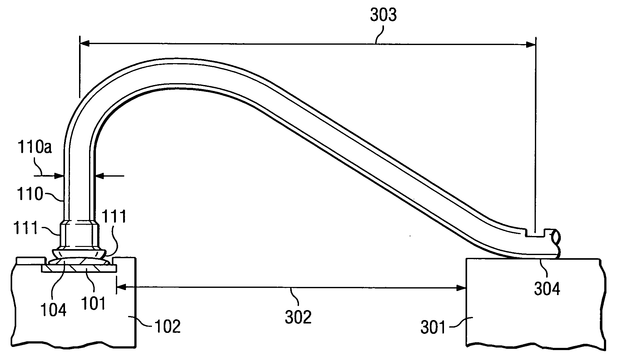
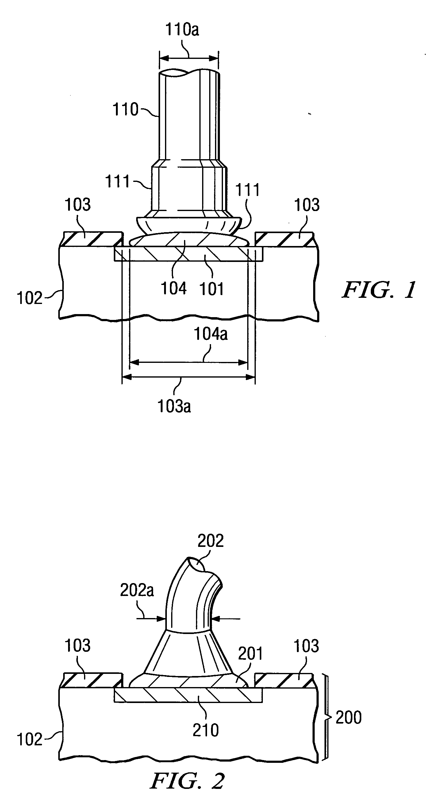
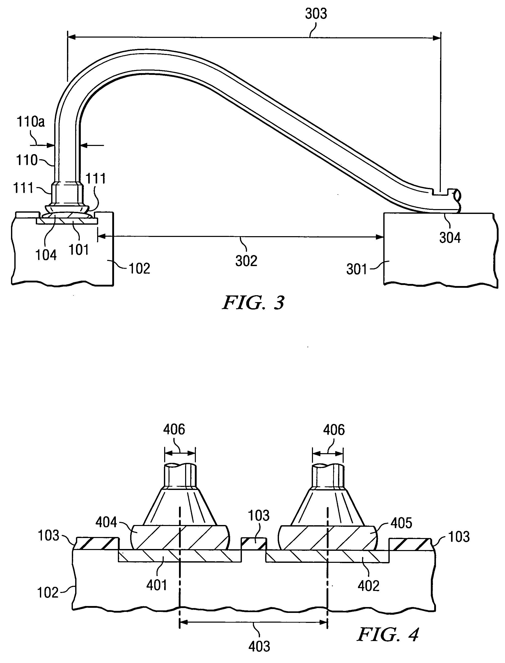
[0021] The schematic cross section of FIG. 1 illustrates a portion on the surface of a semiconductor device, which has a protective overcoat 103, typically consisting of silicon nitride or oxynitride. A window in this overcoat exposes a metallic bond pad 101. The window has a diameter 103a. Bond pad 101 is located over insulating material 102. The bond pad metal 101 may be aluminum or copper, or stacked layers thereof. The insulator 102 may include mechanically weak dielectrics such as silicon-containing hydrogen silsesquioxane (HSQ), aerogels, organic polyimides, parlenes, or alternating layers of plasma-generated tetraethylorthosilicate (TEOS) oxide and HQS, or ozone TEOS oxide and HSQ. The mechanical weakness of these dielectrics, generally referred to as low-k dielectrics, is prone to suffer cracks by mechanical pressure and stress created during the wire bonding operations, but their lower dielectric constant helps to reduce the capacitance C in the RC time constant of circuits...


PUM

PropertyMeasurementUnit
diameteraaaaaaaaaa
temperatureaaaaaaaaaa

Abstract

A semiconductor device with a chip having at least one metallic bond pad (101) over weak insulating material (102). In contact with this bond pad is a flattened metal ball (104) made of at least 99.999 % pure metal such as gold, copper, or silver. The diameter (104a) of the flattened ball is less than or equal to the diameter (103a) of the bond pad. A wire (110) is connected to the bond pad so that the wire has a thickened portion (111) conductively attached to the flattened metal ball. The wire is preferably made of composed metal such as gold alloy. The composition of the flattened ball is softer than the wire. This softness of the flattened ball protects the underlying insulator against damage caused by pressure or stress, when the composed ball is attached.

Description

FIELD OF THE INVENTION [0001] The present invention is related in general to the field of semiconductor devices and processes and more specifically to structure and method of metal bonds to contact pads over dielectrics. DESCRIPTION OF THE RELATED ART [0002] It is well known in semiconductor technology that bond pads on silicon integrated circuits can be damaged during conventional thermosonic wire bonding to circuit bond pad made of aluminum or copper. Mechanical loading and ultrasonic stresses applied by the tip of the bonding capillary to the bond pad are particularly suspect. When the damage is not apparent during the bonding process, the defects may manifest themselves subsequently by succumbing to thermo-mechanical stresses generated during plastic encapsulation, accelerated reliability testing, temperature cycling, and device operation. The damage appears in most cases as microcracks which may progress to fatal fractures in the underlying dielectric, as chip-outs of brittle o...

Claims


Application Information

Patent Timeline
Patent Type & Authority Applications(United States)
IPC IPC(8): B23K31/02
CPCB23K20/005H01L24/45H01L24/48H01L24/85H01L2224/02166H01L2224/05624H01L2224/05647H01L2224/45015H01L2224/45139H01L2224/45144H01L2224/45147H01L2224/4554H01L2224/45565H01L2224/456H01L2224/45647H01L2224/45686H01L2224/48091H01L2224/48247H01L2224/4845H01L2224/48465H01L2224/48475H01L2224/48482H01L2224/48499H01L2224/48624H01L2224/48647H01L2224/48824H01L2224/48847H01L2224/85051H01L2224/85205H01L2924/01006H01L2924/01013H01L2924/01014H01L2924/01029H01L2924/01031H01L2924/01032H01L2924/01047H01L2924/01057H01L2924/01079H01L2924/01205H01L2924/01327H01L2924/10253H01L2924/10271H01L2924/10329H01L2924/14H01L2924/20105H01L2924/20106H01L2924/20107H01L2924/20108H01L2924/20752H01L2924/30105H01L2924/00014H01L2924/00011H01L2924/01019H01L2924/01033H01L2224/78H01L2924/00H01L2224/43848H01L2224/45124H01L2224/48724H01L2224/48747H01L24/43H01L2224/48507H01L2924/181H01L2924/00015H01L2924/01204H01L2924/013H01L2924/01049
Inventor KADOGUCHI, SOHICHIKAWAKAMI, NORIHIRO
Owner TEXAS INSTR INC
Why Eureka
Try Eureka