Vertical organic thin film transistor and organic light emitting transistor

a technology of organic light-emitting transistors and vertical transistors, which is applied in the direction of thermoelectric device junction materials, semiconductor devices, electrical apparatus, etc., can solve the problems of low light-emitting efficiency, high operating voltage of horizontal transistors, and unsuitable use of organic el devices manufactured through active matrix processes, etc., to achieve high light-emitting efficiency

Inactive Publication Date: 2006-07-06
SAMSUNG ELECTRONICS CO LTD
View PDF16 Cites 66 Cited by
  • Summary
  • Abstract
  • Description
  • Claims
  • Application Information

AI Technical Summary

Benefits of technology

[0010] Another object of the embodiments of the present invention is to provide an integrated organic light-emitting transistor, which is formed by forming a light-emitting organic layer having light-emitting properties on the enhancement type organic thin film transistor, thus exhibiting high light-emitting efficiency.

Problems solved by technology

The horizontal transistor has a higher operating voltage and lower efficiency than a vertical transistor, and is unsuitable for use in organic EL devices manufactured through an active matrix process.
Since the operating voltage is low, a battery having small capacity may be used for a long time.
Accordingly, a light-emitting transistor manufactured using the vertical organic transistor is disadvantageous because it has low light-emitting efficiency.

Method used


Image

  • Vertical organic thin film transistor and organic light emitting transistor
  • Vertical organic thin film transistor and organic light emitting transistor
  • Vertical organic thin film transistor and organic light emitting transistor

Examples


example 1

[0045] Fabrication of Vertical Organic Thin Film Transistor Using Copper Phthalocyanine (Cupc)

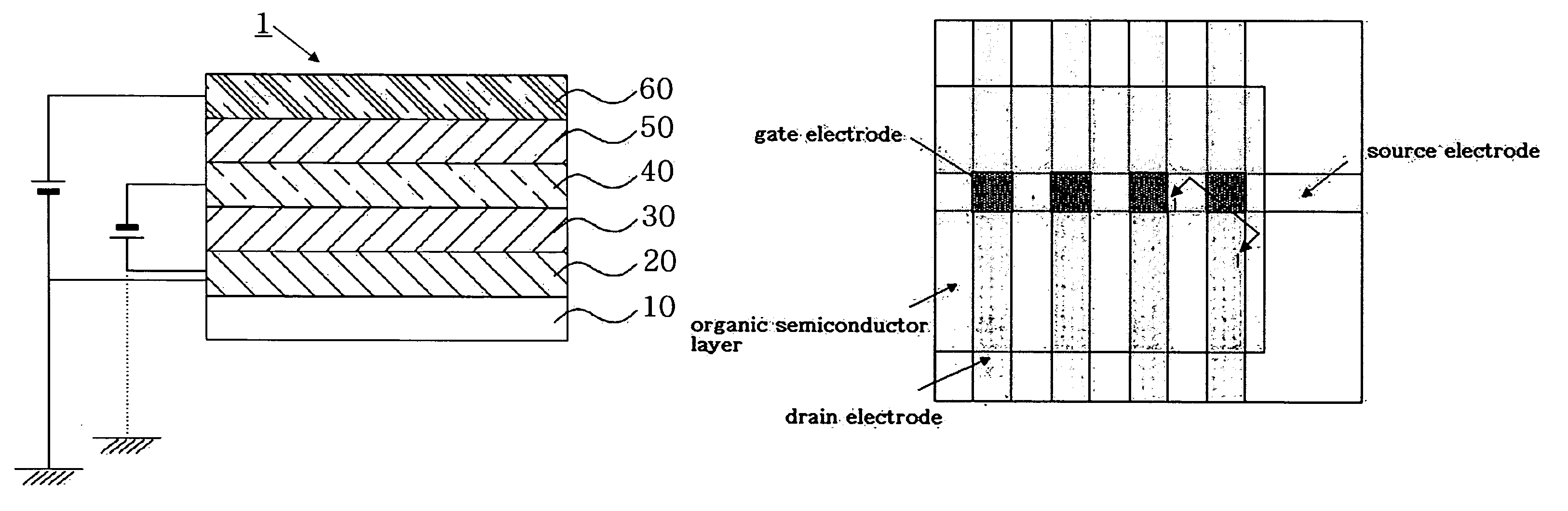
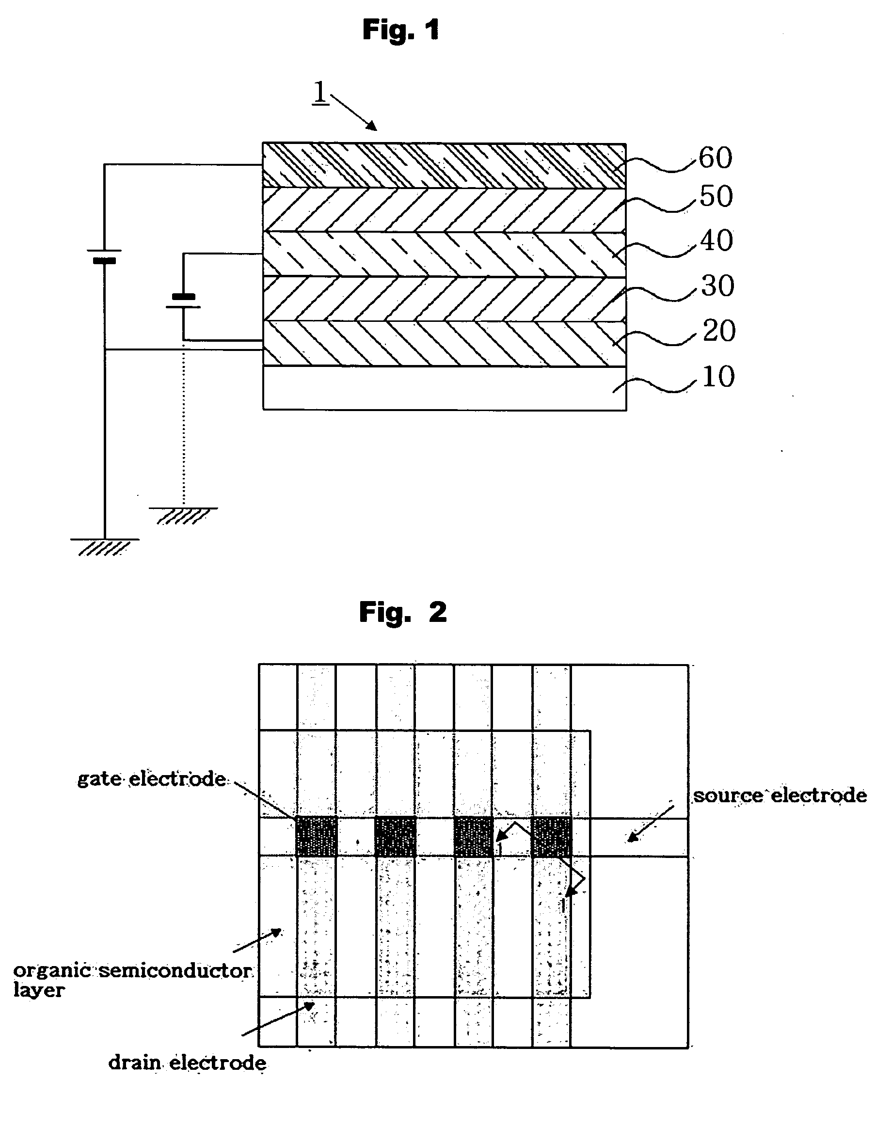
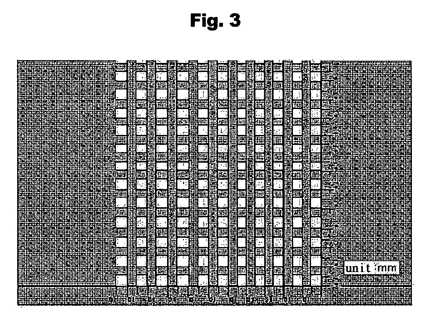
[0046] On a glass substrate coated with ITO, a pattern having a desired shape was formed using a chemical resistant tape. The patterned ITO substrate was dipped into an aqueous solution of hydrochloric acid, after which an unnecessary ITO portion was removed using magnesium powder to obtain the substrate on which only a desired pattern remained, which was then washed with an acetone solvent and dried, thus forming an ITO pattern of a source electrode. On the patterned ITO electrode, copper phthalocyanine was deposited to a thickness of 1000 Å under about 10−5 torr using a vacuum evaporator, to form a first p-type organic semiconductor layer. Subsequently, gate electrodes arranged in a grid shape were deposited to a thickness of 100 Å using a metal mask, as shown in FIG. 3, having a line width of about 100 μm, on the first p-type organic semiconductor layer. Thereafter, a 1000 Å thick secon...

example 2

[0047] Fabrication of Vertical Organic Thin Film Transistor Using Nickel Phthalocyanine (NiPc)

[0048] Chemically patterned ITO, 1000 Å thick nickel phthalocyanine, a 100 Å aluminum electrode, 1000 Å thick nickel phthalocyanine, and a 1000 Å thick aluminum electrode, in that order, were vertically deposited in a vacuum (1×10⁻⁶ torr), thus fabricating a vertical organic thin film transistor. The current-voltage properties of the vertical organic thin film transistor thus obtained were measured. The results are shown in FIGS. 6a and 6b. FIG. 6a shows results at multiple gate voltages, Vg, specifically, at gate voltages of 0, 6, 10, 12, 14, 16, and 20 V.

examples 37

[0049] Respective vertical organic thin film transistors were fabricated in the same manner as in Example 1, with the exception that the structure of the gate electrodes were varied as shown in Table 1, below. The current-voltage properties of the vertical organic thin film transistor thus obtained were measured. The results are shown in Table 1, below.

TABLE 1Ex. No.Gate StructureVds (V)Current (A)On / Off Ratio3Line 0.1 mm, Area: 1 mm210Vg = 0V: 0.253 × 10⁻³ A95.78Vg = 20V: 24.20 × 10⁻³ A4Zipper type, Area: 1 mm210Vg = 0V: 0.107 × 10⁻³ A86.1Vg = 20V: 9.21 × 10⁻³ A5Line 0.1 mm, Area: 4 mm210Vg = 0V: 1.11 × 10⁻³ A78Vg = 20V: 86.80 × 10⁻³ A6Line 0.3 mm, Area: 4 mm210Vg = 0V: 0.492 × 10⁻³ A60Vg = 20V: 29.50 × 10⁻³ A7Grid, Area: 4 mm210Vg = 0V: 0.374 × 10⁻³ A112Vg = 20V: 41.438 × 10⁻³ A


PUM


Abstract

A vertical organic thin film transistor is provided along with an organic light-emitting transistor, which is characterized in that an active layer is formed of a p-type organic semiconductor compound having a dielectric constant of 3.5 or more, and work function values of an anode and a cathode are different from each other. The vertical organic thin film transistor is advantageous because it exhibits excellent current-voltage properties due to a short channel length, and has simple fabrication processes. Also, in the vertical organic thin film transistor, current properties in response to the gate voltage are of an enhancement type. Therefore, the vertical organic thin film transistor may be fabricated into the organic light-emitting transistor through a simple process.

Description

BACKGROUND OF THE INVENTION [0001] This non-provisional application claims priority under 35 U.S.C. § 119(a) on Korean Patent Application No. 2005-00848 filed on Jan. 5, 2005, which is herein expressly incorporated by reference. 1. FIELD OF THE INVENTION [0002] The embodiments of the present invention relate, generally, to a vertical organic thin film transistor and an organic light-emitting transistor using the same. More particularly, the embodiments of the present invention relate to a vertical organic thin film transistor, in which an active layer is formed of a p-type organic semiconductor compound having a dielectric constant of 3.5 or more, and work function values of an anode electrode and a cathode electrode are different from each other, thus exhibiting high current properties, and to an organic light-emitting transistor using such a vertical organic thin film transistor. 2. DESCRIPTION OF THE RELATED ART [0003] Until now, a thin film transistor, which is advantageous beca...

Claims


Application Information

Patent Timeline
Patent Type & Authority Applications(United States)
IPC IPC(8): H01L29/08
CPCH01L27/3244H01L51/0078H01L51/0097H01L51/057H10K59/12H10K85/311H10K10/491H10K77/111H10K10/84
Inventor LEE, SANG YOONKOO, BON WONKANG, IN NAMKIM, CHANG JUOH, SE YOUNG
Owner SAMSUNG ELECTRONICS CO LTD
Why Eureka
Try Eureka