

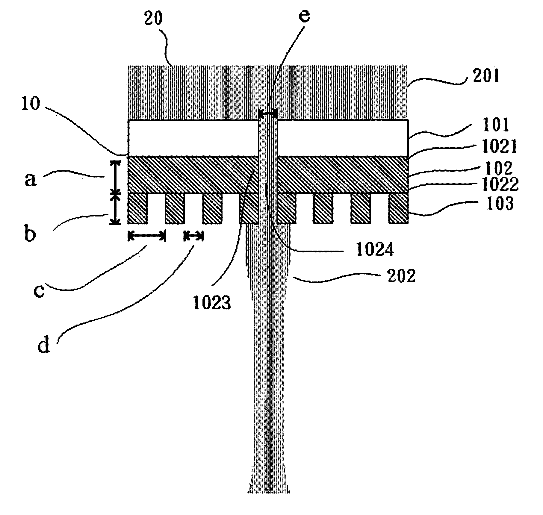
Optical head capable of providing a subwavelength beams
a technology of optical head and beam, which is applied in the field of optical head capable of providing a subwavelength beam, can solve the problems of difficult to further shrink the optical etching linewidth, less material suitable, and different optical applications that face the same difficulties
- Summary
- Abstract
- Description
- Claims
- Application Information
AI Technical Summary
Benefits of technology
Problems solved by technology
Method used
Image

Examples
Embodiment Construction
Explanation of Principle
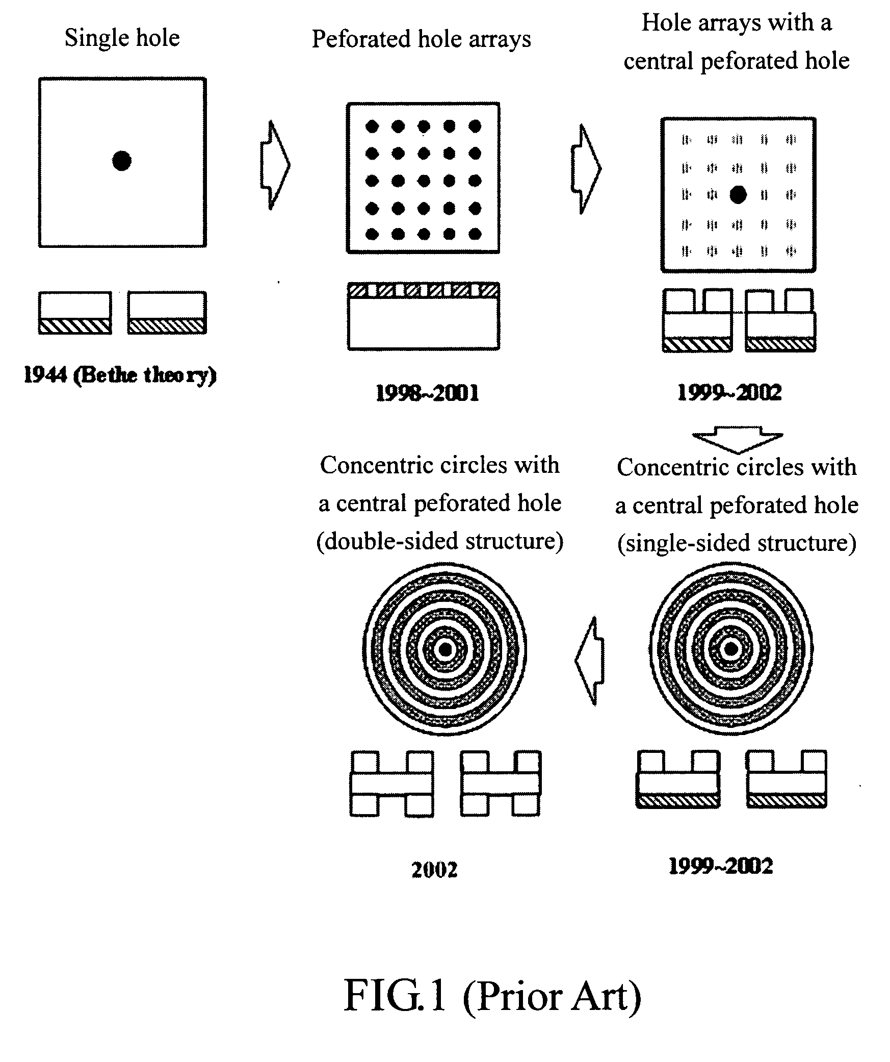
Diffraction Limit of Far Field Optics
[0036] The size of a conventional focusing optical spot is confined by the diffraction limit. In a given wavelength, no matter how to improve performance of an optical system, the focusing optical spot cannot be shrunk to be smaller than a limit, which is proposed by Ernst Abbe in 1884. This limit is based on the principle of diffraction, and called “diffraction limit”.
[0037] The principle of diffraction is briefly described as follows: spatial optical waves can be decomposed to a combination of plane waves in various directions by the fourier optics method. In a specific wavelength, the space frequencies of the plane waves are the same and the difference among them is merely the directions thereof, which can be represented by the equation (1): kx2+ky2+kz2=k2=(2 πλ)2(1)
[0038] Wherein, kx, ky and kz respectively are components of space frequency in X, Y and Z axis.
[0039] Considering a distribution of electric field...
PUM
 Abstract
Description
Claims
Application Information