Electronic devices formed on substrates and their fabrication methods

a technology of electronic devices and substrates, applied in semiconductor devices, transistors, electrical apparatus, etc., can solve problems such as serious problems, errors or trouble of electronic devices due to noise, and limit of silicon devices, and achieve the effect of high resistance to voltag

Inactive Publication Date: 2006-07-20
TAKASHI KATODA
View PDF23 Cites 6 Cited by
  • Summary
  • Abstract
  • Description
  • Claims
  • Application Information

AI Technical Summary

Benefits of technology

[0019] Particularly, the present invention uses as the metal oxide molybdenum oxide which has a bandgap larger than 3.2 eV and is very useful to fabricate electronic devices such as a diode, a bipolar transistor, a field effect transistor and a thyristor with a high withstand voltage. The present invention is also directed to hostile-environment electronic devices composed of high-purity molybdenum oxide.

Problems solved by technology

Although power devices have been fabricated using silicon (Si) for a long time, limits of silicon devices are predicted.
On the other hand, error or trouble of electronic devices due to noise which comes from the cosmic rays or cars and heat has been serious problems.
However there are many additional problems to be solved to realize electronic devices made of GaN or SiC.
One of the most serious problem is that bulk crystal of GaN has not been obtained because an equilibrium vapor pressure of nitrogen is very high relative to that of gallium.
AlN is resistive because it is difficult to dope impurities into AlN.
Use of sapphire substrate in a device which includes multi-layers of semiconductor such as a bipolar transistor and a thyristor is very disadvantageous to their structures and fabrication process.
On the other hand, SiC substrate is very expensive because bulk crystal of SiC can be grown at a very high temperature of 2200˜2400° C. GaN devices using SiC substrate or SiC devices are very expensive.
The problem to be solved realize a new device is to obtain a new substrate which replaces expensive substrate such as sapphire or SiC.
The second serious problem is to realize new devices which can be grown at a lower temperature than that at which GaN or SiC layers are formed.
In addition, there are possibilities that atoms move between layers and a composition is disturbed or dopants move near the interface between layers.
Because the molybdenum plate was not crystal, some fabrication technologies such as cleavage could not used.
Furthermore, precise control of a thickness of the molybdenum oxide layer was difficult when it was formed by oxidation of a molybdenum plate.

Method used


Image

  • Electronic devices formed on substrates and their fabrication methods
  • Electronic devices formed on substrates and their fabrication methods
  • Electronic devices formed on substrates and their fabrication methods

Examples


first embodiment

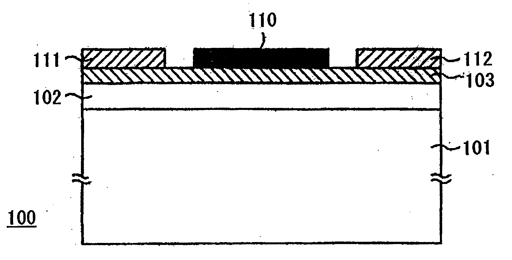
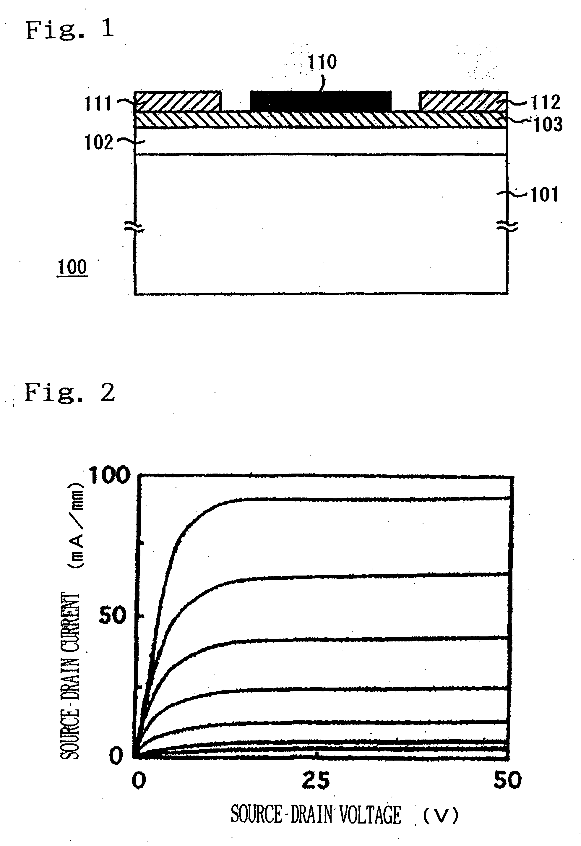
[0033]FIG. 1 is a schematic view of a field effect transistor (100) according to the present invention. In the figure, a substrate (101) is made up of silicon. However, other materials can be used. A layer (102) of molybdenum oxide was formed on the substrate (101). The layer (102) was formed by the following steps. A molybdenum (Mo) plate was used as source and a silicon (Si) substrate were used in this example. At first, the source and the silicon substrate (101) were rinsed and dried. Then they were set in a growth chamber. At the next step, the growth chamber was heated so that a temperature at the source zone was 630° C. and that at the substrate zone was 530° C. under nitrogen atmosphere. After the source and the substrate (101) were heated to the temperatures, respectively, high-purity oxygen was flowed in the growth chamber and kept for 6 hours. A thickness of the layer (102) was 6 μm. Although the layer (102) was not intentionally doped, it was n type with a carrier concent...

second embodiment

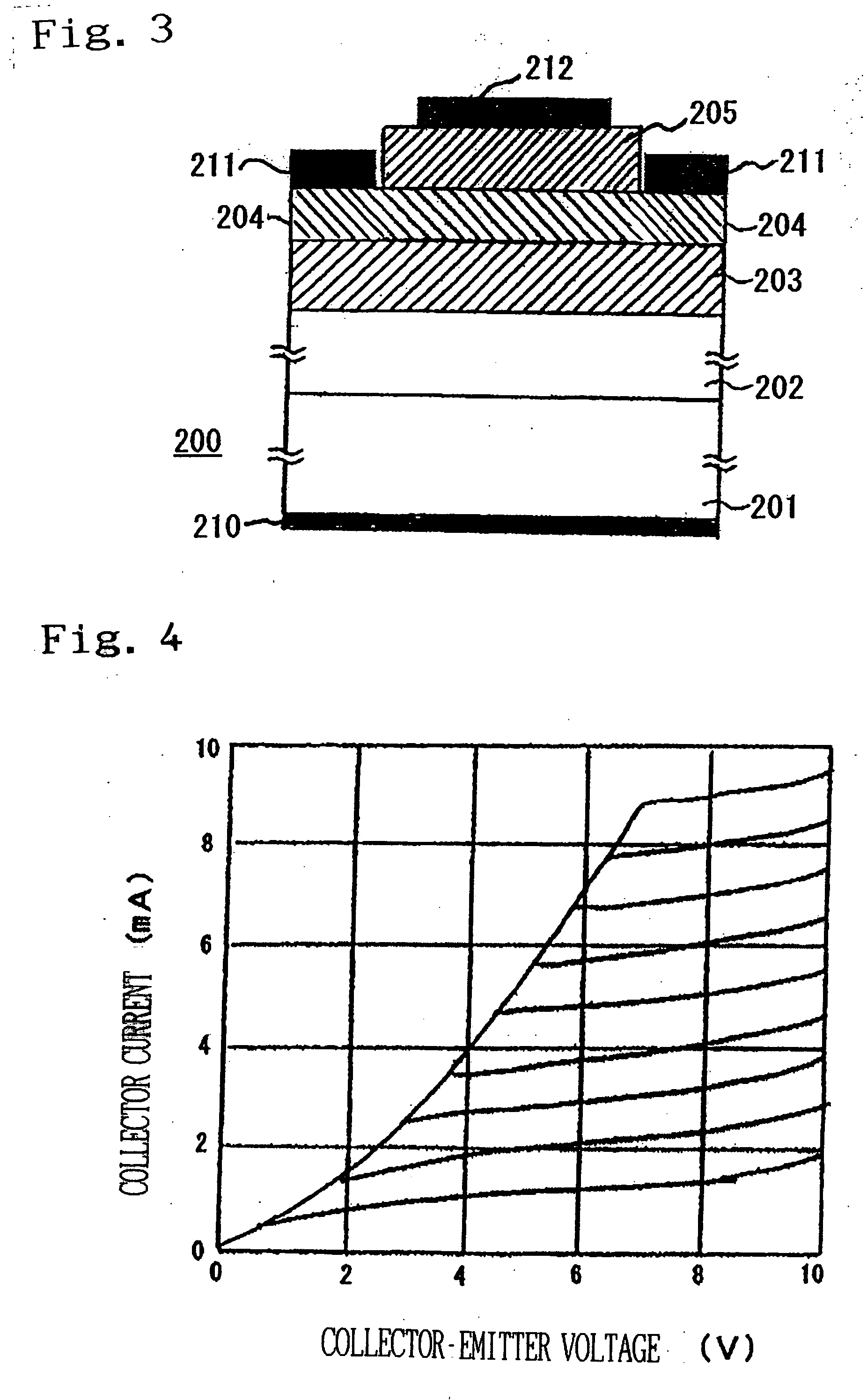
[0037]FIG. 3 is a schematic view of a bipolar transistor (200) according to the present invention. In this embodiment, a substrate (201) consists of silicon. However other materials can be used as a substrate. On the substrate (201) a layer (202) of molybdenum oxide was formed. The layer (202) was formed by the following steps. A molybdenum (Mo) plate was used as source and silicon (Si) substrate were used in this example. At first, the source and the silicon substrate (201) were rinsed and dried. Then they were set in a growth chamber. At the next step, the growth chamber was heated so that a temperature at the source zone was 630° C. and that at the substrate zone was 530° C. under nitrogen atmosphere. After the source and the substrate (201) were heated to the temperatures, respectively, high-purity oxygen was flowed in the growth chamber and kept for 6 hours. A thickness of the layer (202) was 6 μm. Although the layer (202) was not intentionally doped, it was n type with a carri...


PUM


Abstract

The present invention relates to semiconductor electronic devices including molybdenum oxide formed on substrates which consist of materials which are used in known semiconductor electronic devices. The present invention relates to also a new method to fabricate said electronic devices on substrates made of materials which have been used in usual electronic and photonic devices. Suitable substrates consist of materials such as element semiconductors such as silicon and germanium, III-V compound semiconductors such as gallium arsenide and gallium phosphide, II-IV compound semiconductors such as zinc oxide, IV compound semiconductors, organic semiconductors, metal crystals and their derivatives or glasses.

Description

BACKGROUND OF THE INVENTION [0001] 1. Field of the Invention [0002] The present invention relates to semiconductor electronic devices including molybdenum oxide formed on substrates which consist of materials which are used in known semiconductor electronic devices. [0003] More particularly, the present invention relates to field effect transistors, bipolar transistors, thyristors with a high breakdown voltage and hostile-environment electronic devices made up of new semiconductor which can solve difficult problems accompanying to such devices made up of known semiconductors with a large bandgap such as gallium nitride (GaN) and silicon carbide (SiC). [0004] The present invention relates to also a new method to fabricate said electronic devices on substrates made of materials which have been used in usual electronic and photonic devices. [0005] 2. Related Background Art [0006] Recently so-called power devices such as bipolar transistors, field effect transistors, and thyristors are ...

Claims


Application Information

Patent Timeline
Patent Type & Authority Applications(United States)
IPC IPC(8): H01L29/10
CPCH01L29/22H01L29/24H01L29/267H01L29/45H01L29/47H01L29/732H01L29/74H01L29/812H01L29/80
Inventor KATODA, TAKASHI
Owner TAKASHI KATODA
Why Eureka
Try Eureka