Integrated circuit memory devices and capacitors having carbon nanotube electrodes and methods of forming same
- Summary
- Abstract
- Description
- Claims
- Application Information
AI Technical Summary
Problems solved by technology
Method used
Image

Examples
first embodiment
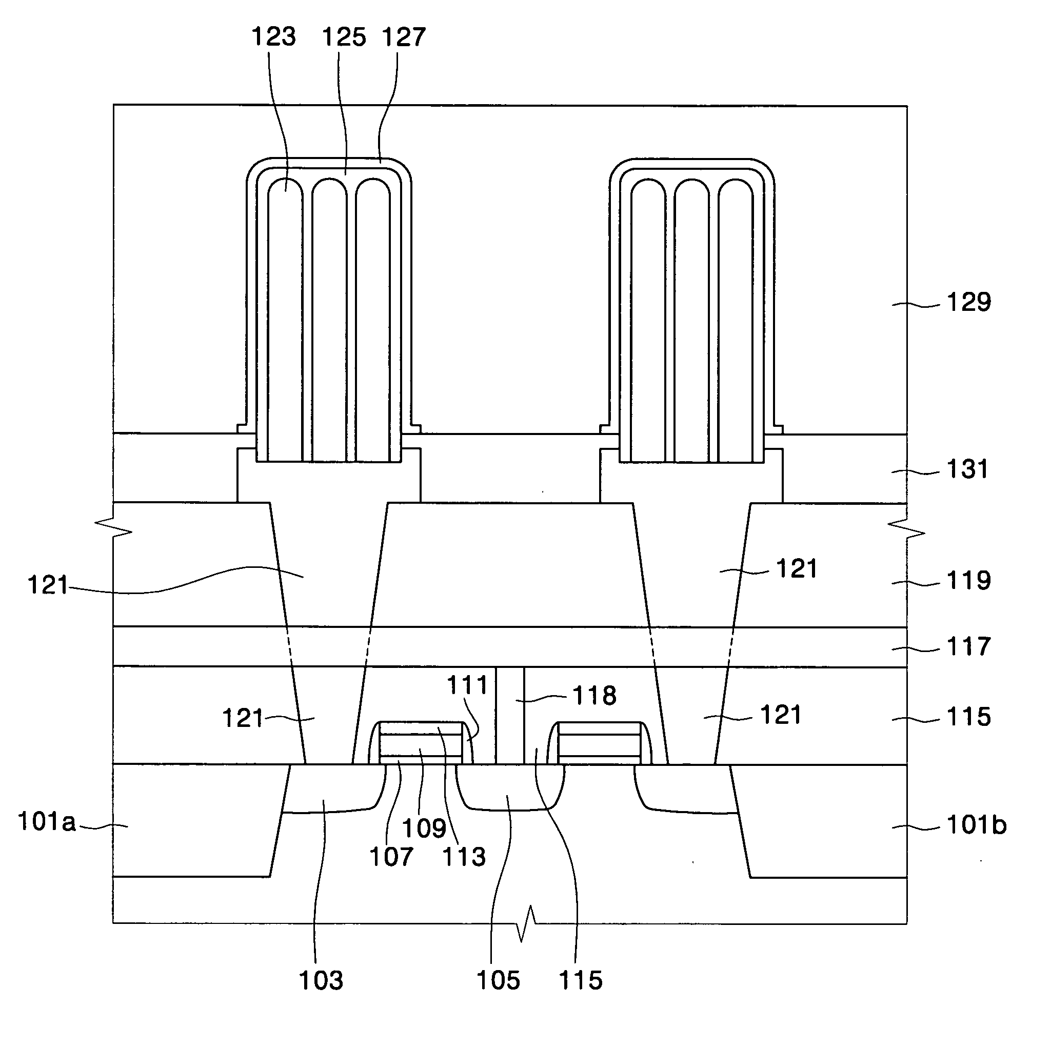
[0012]FIG. 1 is a cross-sectional view illustrating a semiconductor memory device according to the present invention. Referring to FIG. 1, an active region is defined by trenches 101a, 101b formed by shallow trench isolation. A gate is formed on the active region, and a source 103 and a drain 105 are formed in the active region. The source 103 and the drain 105 may be formed by a typical ion implantation process using the gate as an implant. Also, the gate includes a gate oxide film 107 and conduction material 109. Preferably, the gate oxide film 107 is made of SiO2, and the conduction material 109 is made of poly-silicon. The gate may be provided with a sidewall spacer 111 and a hard mask layer 113, which protect the poly-silicon of the gate during subsequent etching processes and doping with a high concentration of ions into the source and drain regions.
[0013] A transistor is defined by the source 103, the drain 105, and the gate provided on the active region. Furthermore, a first...
second embodiment
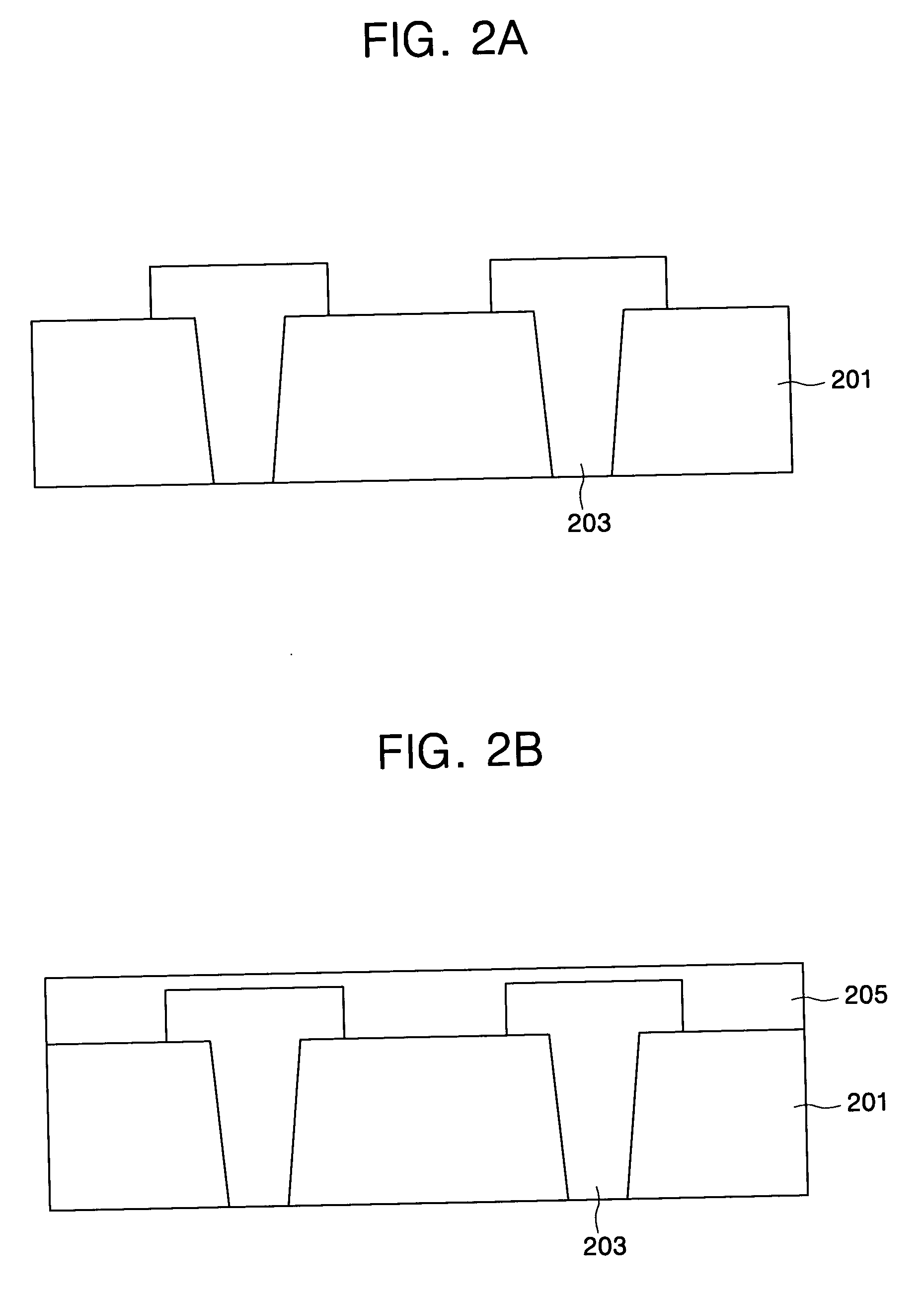
[0017]FIGS. 2A through 2G are cross-sectional views illustrating a method of manufacturing a semiconductor memory device having a single carbon nanotube as a lower capacitor electrode, according to the present invention. Referring to FIG. 2A, a buried contact plug 203 is formed on a semiconductor substrate having a cell transistor, a first interlayer insulating layer (not shown) covering the cell transistor, a bit line (not shown) formed on the first interlayer insulating layer, and a second interlayer insulating layer 201 covering the bit line.
[0018] A buried contact hole is formed in the second interlayer insulating layer 201. The buried contact hole may be formed by depositing a photoresist layer (not shown) on the second interlayer insulating layer 201 and then patterning the photoresist layer by a photolithography process. By the patterning process, predetermined portions of the second interlayer insulating layer 201 are exposed. Then, anisotropic dry etching is applied to the ...
PUM
 Abstract
Description
Claims
Application Information
 - R&D
- Intellectual Property
- Life Sciences
- Materials
- Tech Scout
- Unparalleled Data Quality
- Higher Quality Content
- 60% Fewer Hallucinations
Browse by: Latest US Patents, China's latest patents, Technical Efficacy Thesaurus, Application Domain, Technology Topic, Popular Technical Reports.
© 2025 PatSnap. All rights reserved.Legal|Privacy policy|Modern Slavery Act Transparency Statement|Sitemap|About US| Contact US: help@patsnap.com