Fabrication of advanced silicon-based MEMS devices

a technology of silicon-based mems and fabrication method, which is applied in the direction of television system, instruments, and semiconductor/solid-state device details, can solve the problems of inability to realize the power of mechanical parts, the need to fabricate the integrated circuit after the mechanical parts, and the extra cost of cmp planarization, etc., and achieve the effect of eliminating complex processing

Inactive Publication Date: 2006-07-27
TELEDYNE DIGITAL IMAGING INC
View PDF7 Cites 22 Cited by
  • Summary
  • Abstract
  • Description
  • Claims
  • Application Information

AI Technical Summary

Benefits of technology

[0123] Unlike the prior art, the present invention can produce at a temperature compatible with an underlying integrated circuit an electrically conductive and low mechanical stress and stress gradient laminated structure in a single integrated cycle in a low-temperature reactor without the need for air exposures, without the need for interfacial auxiliary oxide layers, without the need for dopant implantation, without the need for high temperature dopant diffusion and / or activation in a furnace or a rapid thermal processor in order to produce by surface micro-machining over a previously fabricated integrated circuit incorporating CMOS, bipolar, Bi-CMOS and / or high-voltage devices the electrically conductive low-stress mechanical structures allowing the mechanical functions of the integrated MEMS device over its control electronics.
[0124] This integration of modular MEMS devices directly over a previously fabricated integrated circuit is possible because the maximum exposure temperature of 550° C. is now compatible with tungsten-filled contacts and its underlying high quality titanium nitride barrier / glue layer. More, the integration of these modular MEMS devices over an integrated circuit benefit from its smooth surface topology profile and eliminate the complex processing related to the alternate approach requiring extensive planarization of the thick structures composing the MEMS devices as to allow precision photolithography to be performed with modern exposure equipment having small depth of focus.

Problems solved by technology

This is an undesirable combination since advanced integrated circuits require very fine lithography to be performed using short depth-of-focus equipment.
The high-temperature stress-relief restriction, the extra cost associated with CMP planarization, and the need to fabricate the integrated circuit after the mechanical parts are significant restrictions on existing processes.
The integration of moving mechanical parts, of controlling, sensing or interfacing integrated circuits and, sometimes, of high-voltage integrated circuits capable of powerful actuation of the mechanical parts has been so far limited by the high-temperature stress-relief of polysilicon at temperatures exceeding 1000° C.
The resulting 11.8 μm thick structural epipoly layer has a very rough surface (Ra of 260 nm) unacceptable for further processing and thus requiring the use of CMP to reduce the thickness of the structural epipoly layer to 10.3 μm and its surface roughness to about 5 nm.
This is an improvement over the afore-mentioned Prior Art references but, following the integrated circuit fabrication, this process still requires a very restrictive 3 hours duration and 1100° C. stress-relief of the structural polysilicon.
The process is unstable because the compressive stress and surface roughness of the tungsten films are causing processing difficulties, such as delamination, or lifting, of the bondpads and photolithographically instabilities with projection steppers.
A manually-aligned contact aligner has to be used; the TiN diffusion barrier sometimes fail during the 3 hours, 1100° C. stress-relief of the structural polysilicon, thus forming porous WTiSi and WSi at the basis of the contacts; and the out-diffusion of boron from the p+ source / drain implants in silicon causes a severe performance degradation of the p-channel devices due to an increase in contact resistance between tungsten and p-type silicon during the 3 hours, 1100° C. stress-relief of the structural polysilicon;
At this point, it is clear that the restrictive high-temperature stress-relief of the various upper-described popular MEMS processes prevents the integration of the integrated circuit BEFORE the micro-machining steps and prevents any type of modular integration of these micro-machining steps over the integrated circuit.
This high-temperature stress-relief allow the mechanical stress of the electrically conductive polysilicon to be reduced to about 25 MPa but again limits the integration over an integrated circuit.
This described process to achieve doped permeable polysilicon would not be better then University of Michigan's surface micromachining process and would not substantially reduce the stress-relief temperature of the deposited conductive silicon material.
Again, the required four RTA steps at a temperature of about 1000° C. is too restrictive and do not allow MEMS integration AFTER the integrated circuit.
This required RTA or furnace activation at a temperature of about 1000° C. is again too restrictive and do not allow MEMS integration AFTER the integrated circuit.
Because the short duration 950° C. RTA replaces typically longer duration and higher temperature furnace anneals, this technique is slightly better then the upper-discussed techniques but still have a thermal budget which makes the MEMS AFTER the integrated circuit approach unfeasible because the interconnect materials will not resist such a high-temperature stress-relief.
The processes described in the upper prior art documents cannot allow the fabrication of advanced MEMS devices after the integrated circuit because of their excessive high-temperature stress-relief.
The process is yet unstable because of various issues related to: tungsten delamination and lifting at bond pads, tungsten surface roughness imposing manual photolithography, TiN barrier layer failure during the 3 hours, 1100° C. stress-relieve and boron out-diffusion during the 3 hours, 1100° C. stress-relief.
These limitations caused Sandia to drop this idea and look for other approaches besides the all-tungsten, CMOS-first, micromechanics-last MEMS process.
None of the cited prior art references described a process which can allow the effective fabrication of advanced MEMS devices after the integrated circuit because to each of these are associated an excessive high-temperature treatment to stress-relief, dope or activate the dopants of the deposited silicon.

Method used


Image

  • Fabrication of advanced silicon-based MEMS devices
  • Fabrication of advanced silicon-based MEMS devices
  • Fabrication of advanced silicon-based MEMS devices

Examples


Embodiment Construction

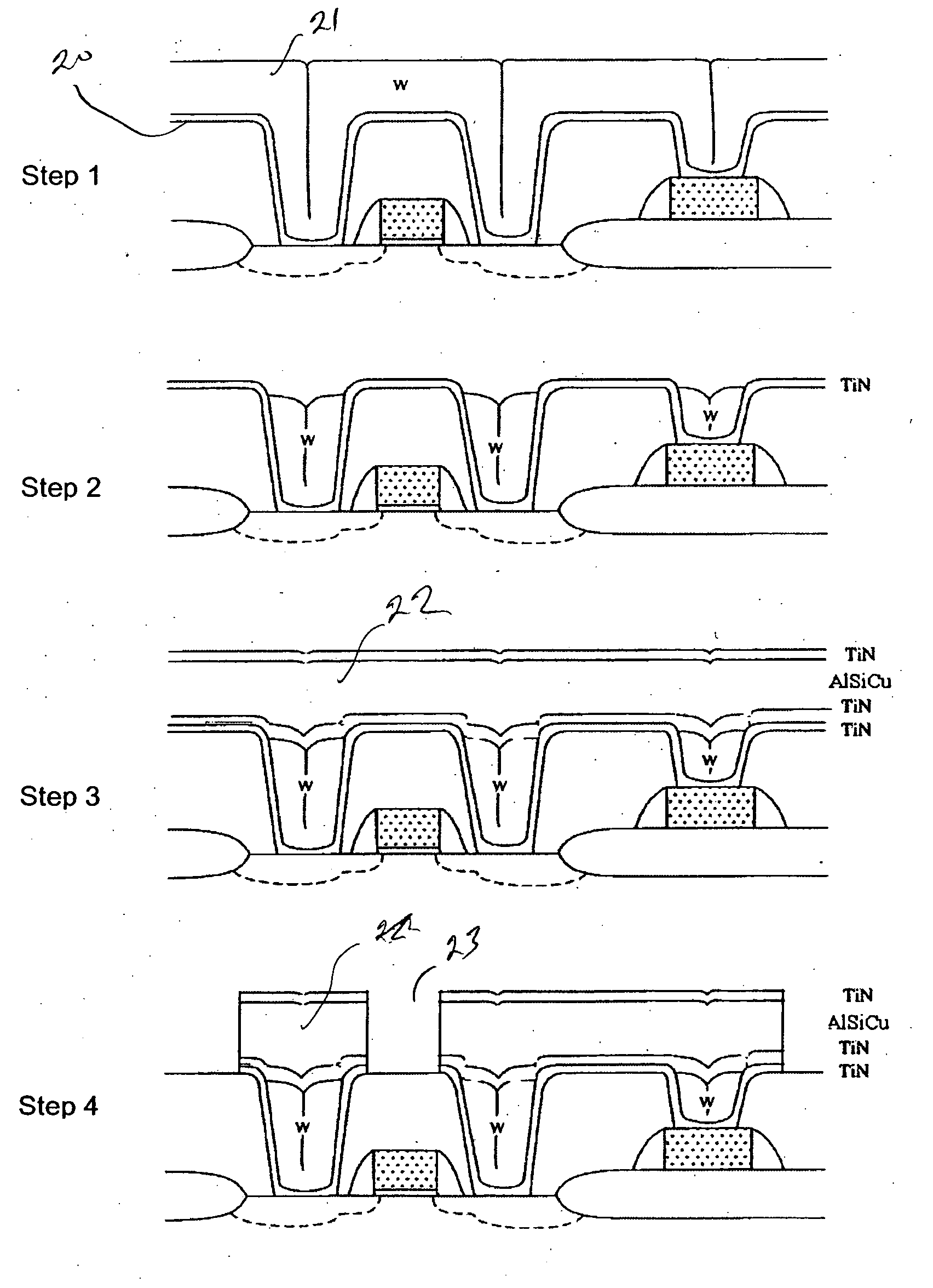
[0153] The process allowing the fabrication of advanced MEMS devices after the integrated circuit is shown in FIG. 11. This process requires the mechanical parts of the MEMS device to be fabricated over the interconnections of the integrated circuit, thus imposing an upper limit on the process temperature of about 550° C., the maximum temperature at which aluminium interconnections can be exposed.

[0154] The MEMS device shown in FIG. 11 has a mechanical MEMS part 10 and an integrated circuit part 11. These are formed on a silicon substrate 12 having a well 13 with tungsten plugs 14 over Ti / TiN at the contacts. A TiN / Al / TiN layer 15 provides the interconnects.

[0155] A first silicon layer 15 interconnects the integrated circuit 11 and MEMS device 10, which is made out of structural silicon layers 17 over a region 18 where sacrificial material has been removed.

[0156] The maximum temperature at which typical Al—Si binary alloy, Al—Cu binary alloy or Al—Si—Cu ternary alloy interconnect...


PUM


Abstract

A micro-electro-mechanical (MEM) device and an electronic device are fabricated on a common substrate by fabricating the electronic device comprising a plurality of electronic components on the common substrate, depositing a thermally stable interconnect layer on the electronic device, encapsulating the interconnected electronic device with a protective layer, forming a sacrificial layer over the protective layer, opening holes in the sacrificial layer and the protective layer to allow the connection of the MEM device to the electronic device, fabricating the MEM device by depositing and patterning at least one layer of amorphous silicon, and removing at least a portion of the sacrificial layer. In this way, the MEM device can be fabricated after the electronic device on the same substrate.

Description

CROSS REFERENCE TO RELATED APPLICATIONS [0001] This application claims the benefit under 35 US 119(e) of prior U.S. provisional applications Ser. No. 60 / 445,426 filed Feb. 7, 2003 and Ser. No. 60 / 447,019 filed Feb. 13, 2003.FIELD OF THE INVENTION [0002] This invention relates to the fabrication of MEMS (Micro-Electro-Mechanical Systems) devices, and more particularly to a method of fabricating MEMS devices that permits the fabrication of advanced integrated circuits prior to the fabrication of the mechanical components on the same device. BACKGROUND OF THE INVENTION [0003] The production of advanced silicon-based micro-electro-mechanical systems, MEMS, requires the integration of moving mechanical parts and controlling, sensing or interfacing integrated circuits, and sometimes high-voltage integrated circuits capable actuating the mechanical parts. [0004] The processes used to produce advanced MEMS from silicon-based structural materials typically require a high-temperature stress-r...

Claims


Application Information

Patent Timeline
Patent Type & Authority Applications(United States)
IPC IPC(8): H01L21/50H01L21/48H01L21/44B81B3/00B81B7/00B81B7/02B81C99/00H01L21/8242
CPCB81C1/00246B81C1/00666B81C2201/0164B81C2201/0167B81C2201/0169B81C2203/0735
Inventor OUELLET, LUCANTAKI, ROBERT
Owner TELEDYNE DIGITAL IMAGING INC
Why Eureka
Try Eureka