Thin film processing method and thin film processing apparatus

a technology of thin film and processing method, which is applied in the direction of gel state instruments, manufacturing tools, etc., can solve the problems that the connection pitch of the tab connection or the wire bonding method cannot be significantly reduced, the uniformity of polycrystalline silicon thin film transistors cannot be satisfied, and the low softening point glasses cannot be employed. achieve satisfactory properties and good quality

Inactive Publication Date: 2006-08-24
NEC CORP +1
View PDF1 Cites 18 Cited by
  • Summary
  • Abstract
  • Description
  • Claims
  • Application Information

AI Technical Summary

Benefits of technology

[0049] Next, the case where a delayed second laser light is irradiated with a delay relative to a first laser light. As is described above, a laser light at a late light emission stage suppresses the increase of the cooling rate, and the cooling rate after the completion of light emission controls the crystallization. The last supplied energy is supposed to initialize precedent cooling processes. Specifically, by supplying an additional energy, a precedent cooling process is once initialized and a solidification process is repeated again, even if the crystal becomes amorphous or microcrystalline in the precedent cooling process. This is provably because the interval of light irradiation is very short of the order of nanoseconds, and loss of the energy by thermal conduction to the substrate and radiation to the atmosphere is small. The energy previously supplied therefore remains nearly as intact. In this assumption, a long time interval sufficient to dissipate heat is not considered. Accordingly, by controlling the cooling rate after the completion of a second heating by the additionally supplied energy, the crystal is expected to grow satisfactorily. As shown in FIG. 14, the cooling rate is controlled to a desired level by controlling the delay time of the second laser irradiation.

Problems solved by technology

A conventional tab connection method or wire bonding method cannot significantly provide such a decreased connection pitch.
However, if a process at high temperatures as in the above case is employed in the polycrystalline silicon TFT process, low softening point glasses cannot be employed.
The resulting polycrystalline silicon thin film and polycrystalline silicon thin film transistor cannot therefore have satisfactorily uniform characteristics.
However, according to this process, a weak light is rather oscillated even though the formation of spiking is inhibited.
The resulting transistor element and thin film integrated circuit cannot have a significant uniformity in the substrate plane.
However, this technique shown in FIG. 16(2) cannot be applied to a process of intermittently repeating the lasing and the movement of stage.
However, although this process can stably irradiate the substrate with a laser beam, the process also yields increased excess lasing that does not serve to the formation of a polycrystalline silicon thin film.
The productivity is decreased from the viewpoint of the life of an expensive laser source and an excited gas, and the production efficiency of the polycrystalline silicon thin film is deteriorated with respect to power required for lasing.
The production costs are therefore increased.
When a substrate to be exposed to laser is irradiated with an excessively strong light as compared with a target intensity, the substrate will be damaged.
Such an excessively strong light is induced by an irregular irradiation intensity.
In LCDs and other imaging devices, a light passing through the substrate scatters in an area where the substrate is damaged, and the quality of image is deteriorated.
However, as pointed out in the above reference, such an increased irradiation energy invites the resulting film to become amorphous or microcrystalline.
Particularly, when the cooling rate in cooling procedure is extremely large and the material undergoes an excessive supercooling, the material is not crystallized at around its solidification point, and becomes an amorphous solid due to quenching and rapid solidification.

Method used


Image

  • Thin film processing method and thin film processing apparatus
  • Thin film processing method and thin film processing apparatus
  • Thin film processing method and thin film processing apparatus

Examples


Embodiment Construction

[0069] The embodiments of the invention will now be illustrated in detail with reference to the drawings.

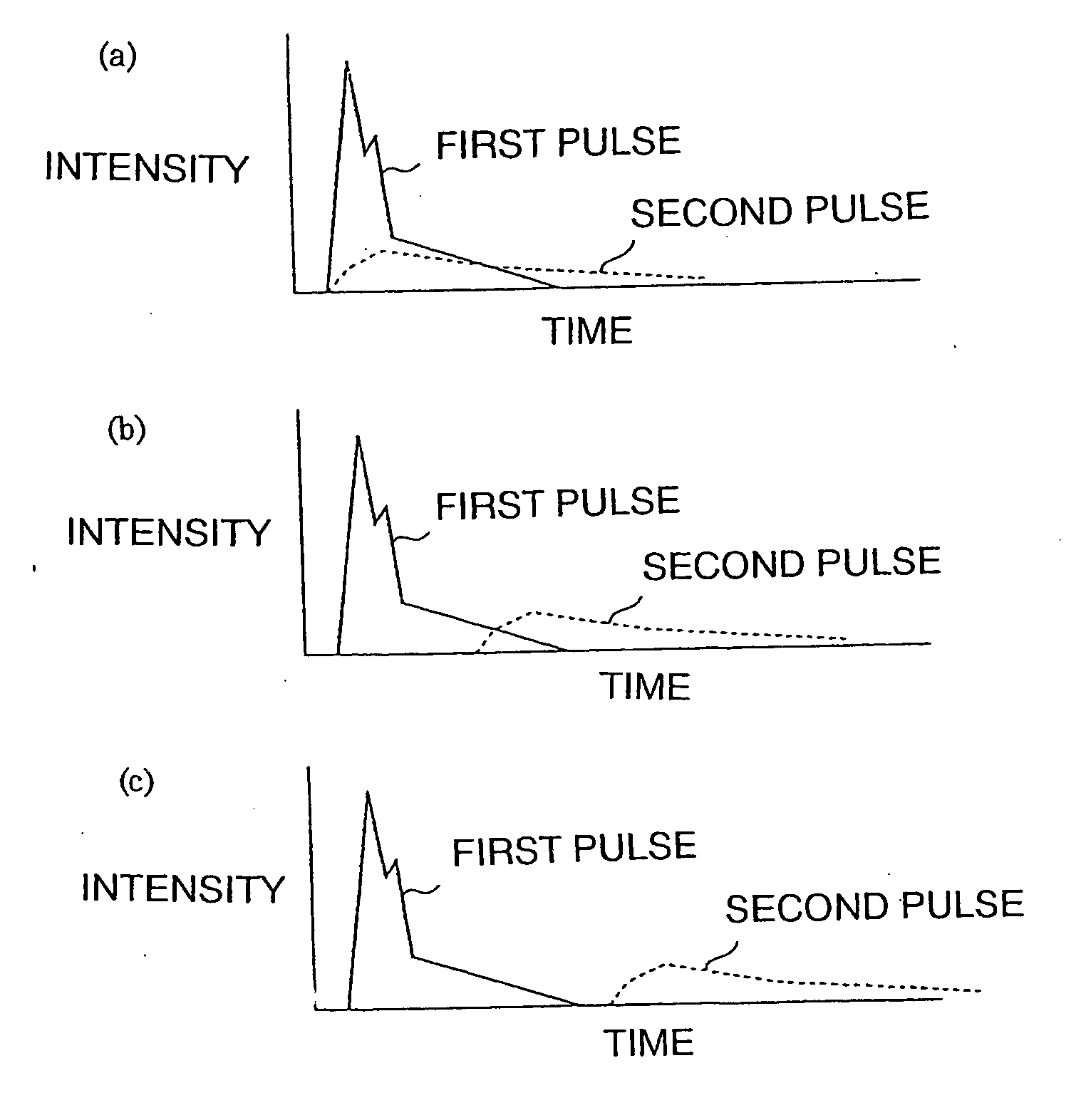
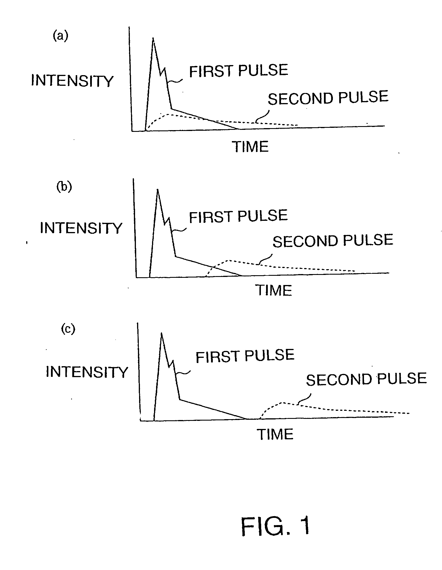
[0070]FIG. 1 illustrates an example of the embodiment of the present invention. Each of the oscillation start timings is depicted as the abscissa axis while the irradiation energy is depicted as the region bound by the pulse line. FIG. 1(a) shows an example where a first pulse laser and a second pulse laser are oscillated at the simultaneous timing. The time interval required between the supply of the trigger signal for controlling the oscillation and the actual start of the oscillation often depends upon the construction of the laser apparatus. Therefore, the “trigger oscillation” time is predetermined so that the irradiation can be simultaneously carried out. Since the emission time of the second pulse is longer than that of the first pulse, the gradual-cooling effect becomes higher during the melting and solidifying process. Moreover, during the melting process by the first p...


PUM

PropertyMeasurementUnit
temperatureaaaaaaaaaa
temperaturesaaaaaaaaaa
sizeaaaaaaaaaa

Abstract

A thin film processing method for processing the thin film by irradiating an optical beam to the thin film. A unit of the irradiation of the optical beam includes a first and a second optical pulse irradiation to the thin film, and the unit of the irradiation is carried out repeatedly to process the thin film. The first and the second optical pulse have pulse waveforms different from each other. Preferably, a unit of the irradiation of the optical beam includes the a first optical pulse irradiated to the thin film and a second optical pulse irradiated to the thin film starting substantially simultaneous with the first optical pulse irradiation. In this case, the relationship between the first and the second optical pulse satisfies (the pulse width of the first optical pulse)<(the optical pulse of the second optical pulse) and (the irradiation intensity of the first optical pulse)≧(the irradiation intensity of the second optical pulse). A silicon thin film with a small trap state density can be formed by the optical irradiation.

Description

[0001] This is a divisional of application Ser. No. 10 / 275,692, filed on Jul. 2, 2003. The entire disclosure of which is hereby incorporated by reference.BACKGROUND OF THE INVENTION [0002] 1. Field of the Invention [0003] This invention relates to a system for the formation of a silicon thin film and a good-quality semiconductor-insulating film interface. Such silicon thin films are used for crystalline silicon thin film transistors, and such semiconductor-insulating film interfaces are employed for field effect transistors. The invention also relates to a semiconductor thin film forming system by the pulsed laser exposure method. In addition, the invention relates to a system for the manufacture of driving elements or driving circuits composed of the semiconductor thin films or field effect thin film transistors for displays and sensors, for example. [0004] 2. Description of the Related Art [0005] Typical processes for the formation of a thin film transistor (TFT) on a glass substr...

Claims


Application Information

Patent Timeline
Patent Type & Authority Applications(United States)
IPC IPC(8): H01L21/48B23K26/00H01L21/20H01L21/208H01L21/268H01L21/336H01L29/786
CPCH01L21/2026H01L21/268H01L29/66757H01L29/78675H01L21/02532H01L21/0262H01L21/02686H01L21/31
Inventor TANABE, HIROSHITANEDA, AKIHIKO
Owner NEC CORP
Why Eureka
Try Eureka