Methods for using resonant waveguide-grating filters and sensors

a technology of resonant waveguide and filter, applied in the field of optical filters and sensors, can solve the problem that the substance to be sensed may not efficiently attach to the dielectric material

Inactive Publication Date: 2006-08-31
BOARD OF RGT THE UNIV OF TEXAS SYST
View PDF23 Cites 171 Cited by
  • Summary
  • Abstract
  • Description
  • Claims
  • Application Information

AI Technical Summary

Benefits of technology

[0014] In another respect, the invention is a system for spectral filtering and the system utilizes a guided-mode resonance effect in a waveguide. The guided-mode resonance effect is described below in greater detail. The system includes a waveguide grating device. The waveguide grating device includes at least one waveguide that has a proximal end and a distal end. The distal end of the at least one waveguide has an endface. The device also has a waveguide grating fabricated on the endface of the at least one waveguide. The waveguide grating has at least one waveguide layer and at least one grating layer. The waveguide grating also has a plurality of variable parameters. The plurality of variable parameters includes at least one permittivity of the at least one grating layer, the permittivity of the at least one waveguide layer, the periodic structure of the at least one grating layer, the grating fill factor of the at least one grating layer, the thickness of the at least one waveguide layer, and the thickness of the at least one grating layer. The at least one waveguide layer and the at least one grating layer may be the same layer. Also, the permittivity of the at least one waveguide layer and one of the permittivities of the at least one permittivity of the at least one grating layer may be the same.

Problems solved by technology

In some cases, the substance to be sensed may not attach itself efficiently to dielectric materials composing, at least in part, the waveguide grating.

Method used


Image

  • Methods for using resonant waveguide-grating filters and sensors
  • Methods for using resonant waveguide-grating filters and sensors
  • Methods for using resonant waveguide-grating filters and sensors

Examples


example 1

[0082] Example I describes a procedure that was undertaken to optimize the manner of fabricating a diffractive grating, but not a waveguide grating, on the endface of a fiber. A high quality cleaving tool was used to obtain flat, optical quality endfaces on both single-mode and multimode fibers. After cleaving, the fibers were visually inspected with an optical microscope to determine endface quality. The fibers were cleaned by immersion in an ultrasonic bath of heated acetone for 30 minutes, briefly dipped in optical grade methanol, and dried with filtered nitrogen gas.

[0083] The fabrication procedure was initially optimized by recording efficient submicron diffractive structures on the optical fiber endfaces. Thin films of UV-sensitive Shipley 1805 photoresist (PR) were deposited on the cleaved multimode and single-mode fiber endfaces by a dipping process. It was found that a dilution of 3 parts PR to 5 parts Shipley photoresist thinner yielded an approximate PR thickness of 300 ...

example 2

Fabrication of Waveguide Gratings on Endfaces of Waveguides

[0086] In this example, waveguide gratings were fabricated on the endfaces of optical fibers. Once the ends of the fibers were cleaved to form endfaces and cleaned, deposition of dielectric thin-films was required to create a waveguide grating structure. In this example, thin films of Si3N4 were deposited by sputtering on the clean, uncoated optical fiber endfaces. Silicon nitride is a hard, low loss dielectric material that has a relatively high refractive index (n=2.0). This commonly-used coating can also be patterned by etching in a reactive ion etching (RIE) chamber using standard fluorocarbon etchant gases, such as CF4 or CHF3. An RF-powered sputter machine that housed a single, three-inch Si3N4 target was used to deposit the nitride films. Inert argon gas was used as the primary sputter gas, with a small amount (˜5%) of N2 included to prevent nitrogen depletion of the Si3N4 target. Nitrogen depletion results in an Si-...

example 3

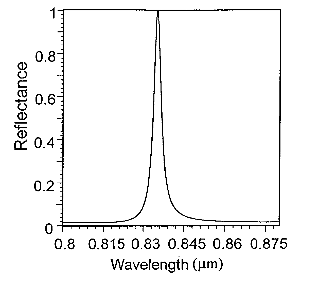
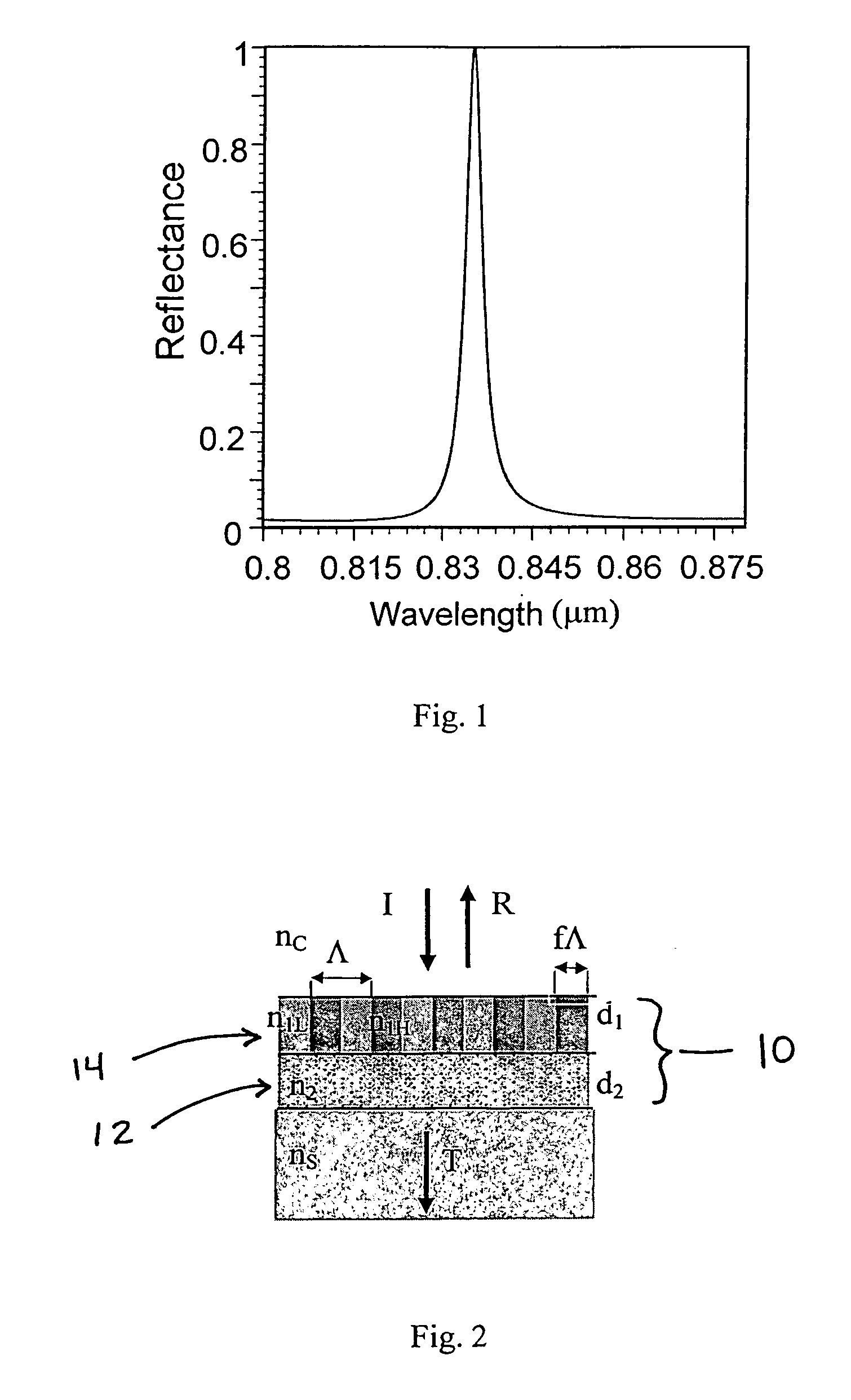
[0088]FIG. 4 depicts calculated TE and TM polarization spectral responses of a waveguide grating with the cross section shown in FIG. 5, having the following parameters: grating period, Λ, is 0.51 μm; thickness, d1, is 0.4 μm; thickness, d2, is 0.18 μm; refractive index, nH, is 1.63; refractive index, nL, is 1.0; refractive index, n2, is 1.9; and refractive index, nS, is 1.45. The calculations leading to the results depicted in FIG. 4 were performed with rigorous coupled-wave analysis, assuming plane waves at normal incidence on a structure with an infinite number of grating periods.

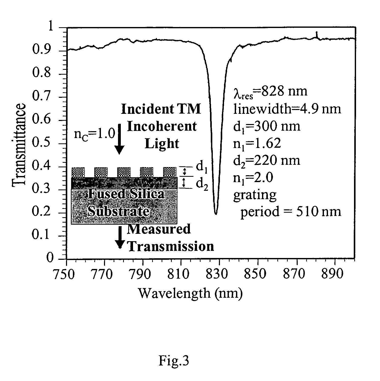
[0089] Turning now to the details of this experiment, ˜200 nm layers of Si3N4 were sputter deposited on multimode optical fiber endfaces with 100 μm core diameters. PR gratings with 510 nm periods were subsequently recorded to yield waveguide grating devices. The parameters of the devices are as follows: grating period, L, is 510 nm; PR thickness, d1, is 300 nm; Si3N4 thickness, d2, is 200 nm; refractiv...


PUM


Abstract

Methods of detecting one or more parameters of a medium are disclosed. The methods include providing a waveguide grating device, contacting the waveguide grating with a medium, propagating a signal having at least one signal attribute through the waveguide, and comparing the modified signal attribute to a known signal attribute to detect a parameter of the medium.

Description

CROSS-REFERENCES TO RELATED APPLICATIONS [0001] This is a divisional of co-pending application Ser. No. 09 / 707,435, filed Nov. 6, 2000, which claims priority to U.S. Provisional Patent Application Ser. No. 60 / 163,705 filed Nov. 5, 1999 and U.S. Provisional Patent Application Ser. No. 60 / 164,089 filed Nov. 6, 1999. The entire texts of these provisional patent applications are specifically incorporated by reference without disclaimer.BACKGROUND OF THE INVENTION [0002] 1. Field of the Invention [0003] The present invention relates generally to the field of optical filters and sensors. More particularly, it concerns the use of the guided-mode resonance effect occurring through the use of waveguide gratings attached to the endfaces of waveguides such as optical fibers in fields such as optical sensing and communications. [0004] 2. Description of Related Art [0005] Resonance anomalies occurring in waveguide gratings (WGGs) have been the subject of current interest for spectral filtering a...

Claims


Application Information

Patent Timeline
Patent Type & Authority Applications(United States)
IPC IPC(8): G02B6/00
CPCG01N21/648G01N21/7743G01N2021/7776G02B6/02061G02B6/29317G02B2006/12107G02B6/34
Inventor WAWRO, DEBRA D.TIBULEAC, SORINMAGNUSSON, ROBERT
Owner BOARD OF RGT THE UNIV OF TEXAS SYST
Why Eureka
Try Eureka