

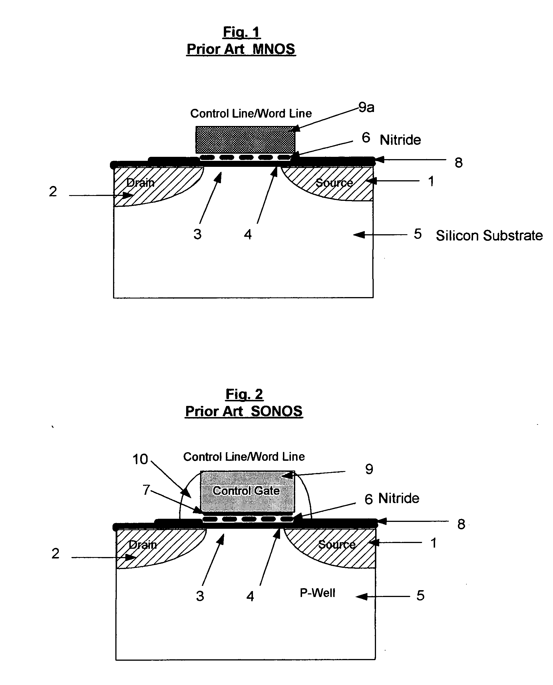
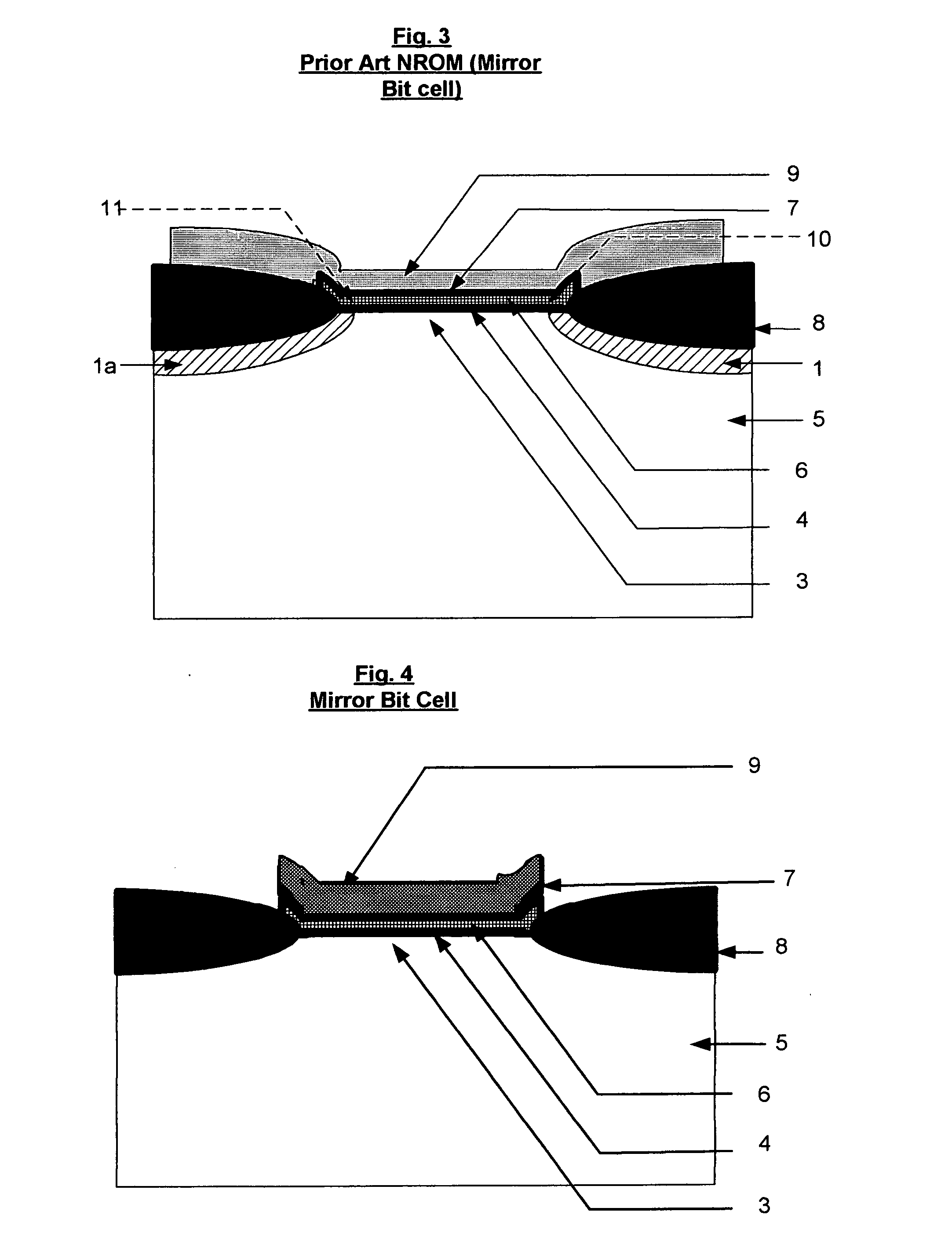
Nitride storage cells with and without select gate
a nitride and memory cell technology, applied in the direction of semiconductors, electrical devices, transistors, etc., can solve the problems of difficult if not impossible, large needed voltage for this type of operation, and the use of not too well controlled phenomena requires critical drain engineering, etc., to achieve high density and embedded nvm
- Summary
- Abstract
- Description
- Claims
- Application Information
AI Technical Summary
Benefits of technology
Problems solved by technology
Method used
Image

Examples
Embodiment Construction
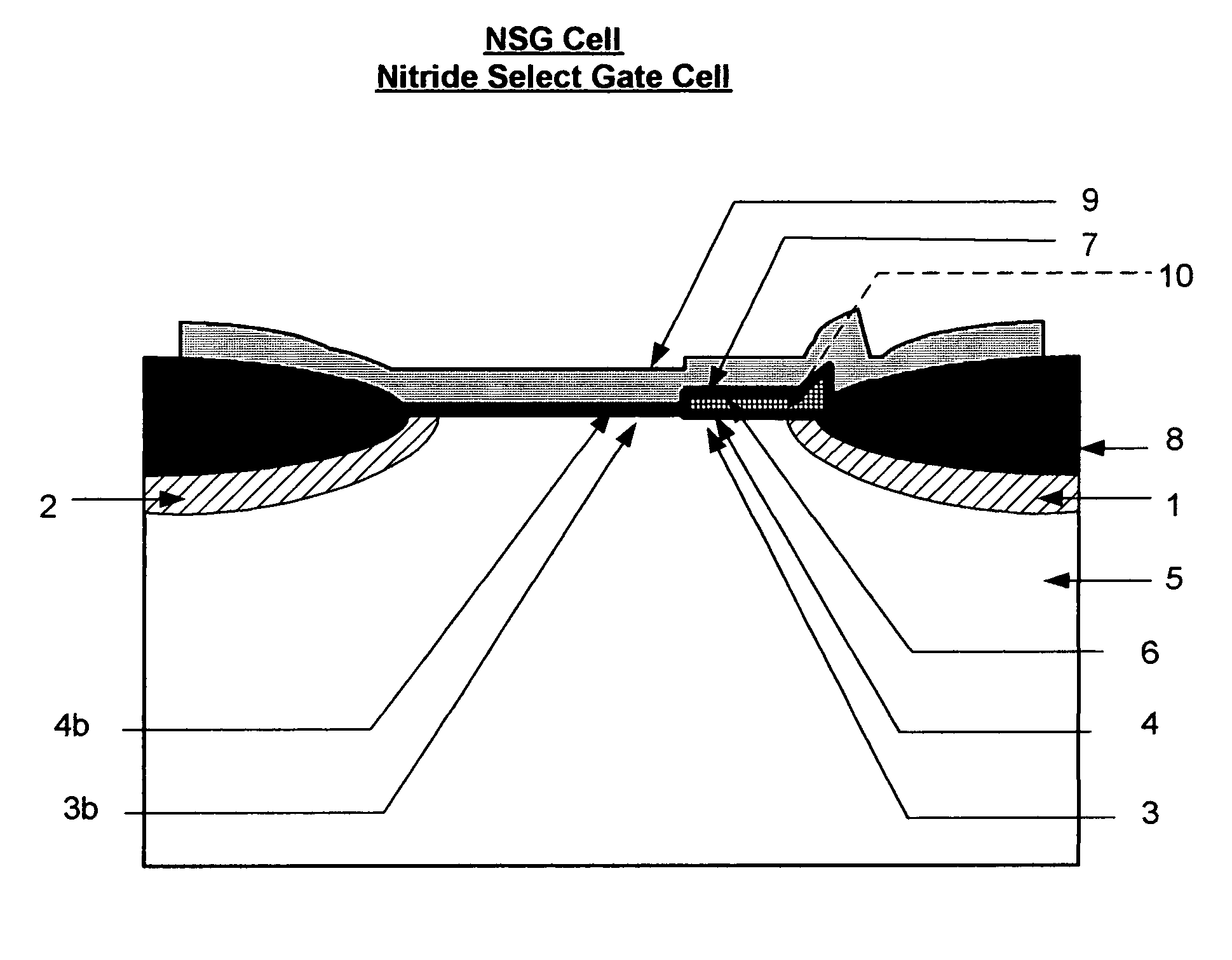
[0102]FIG. 5 shows the cross section of a NSG device with buried channel source / Drain diffusions (1) and (2) contacts and FIG. 6 is the orthogonal cross section of the same device through the Nitride gate region. The self aligned ONO sandwich with Oxide (4), Nitride layer (6), and top oxide layer (7) form the storage element with the charge being stored in traps in the Nitride (6). This structure is deposed over a silicon material (5) having a well doping of typically P type, adjacent one Source / Drain diffusion typically (10 as shown in FIG. 5. The isolation oxide regions (8) are formed using the Nitride film before the film is etched off from the region where the select gate oxide (4b) is formed. A Poly-silicon film over lying the ONO and the Gate Oxide form the integrated control gate / Select Gate conductor (9). As shown in FIG. 5 the select gate is integrated with the storage gate and the integrated channel (4 and 4b) extends from one typically n-type diffusion to the other. The s...
PUM
 Abstract
Description
Claims
Application Information