
Method for manufacturing field effect transistor

a field effect transistor and manufacturing method technology, applied in the direction of basic electric elements, electrical appliances, semiconductor devices, etc., to achieve the effects of improving characteristics, reducing threshold voltage, and enhancing diffusion of impurities

Inactive Publication Date: 2006-09-07
RENESAS ELECTRONICS CORP
View PDF14 Cites 4 Cited by
  • Summary
  • Abstract
  • Description
  • Claims
  • Application Information

AI Technical Summary

Benefits of technology

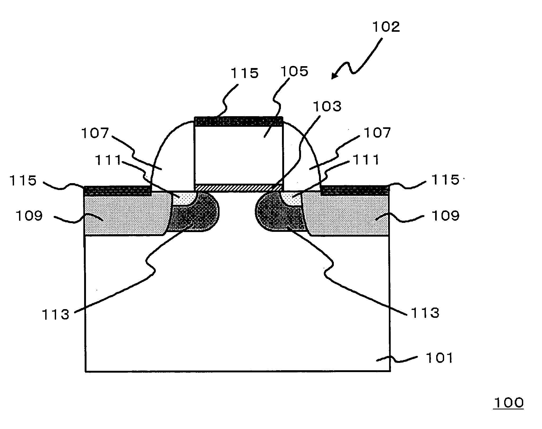
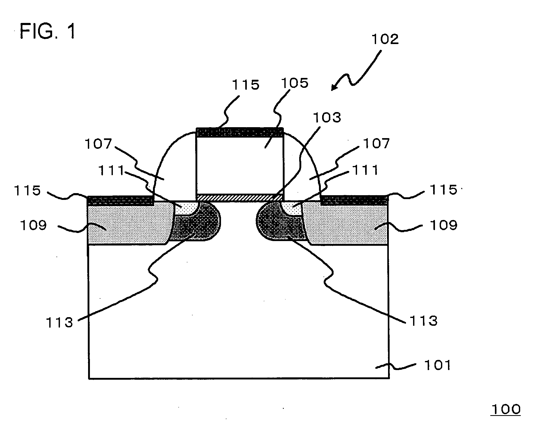
[0056] Next, advantageous effects obtainable by employing the configuration of the semiconductor device 100 shown in FIG. 1 will be described. In the semiconductor device 100, the n-type MOSFET 102 is manufactured by conducting a FLA process (S103 and S105 in FIG. 4) as a process for eliminating defects created in the ion implantation process between the process for ion-implanting to the silicon substrate 101 and a heating process that is the earliest heating process conducted thereafter. More specifically, the FLA of step 103 is conducted after the ion implantation into the n-type extension region 111 in step 102 and before the heating process conducted during the process for forming the side wall insulating film 107. Further, after the ion implantation into the n-type source / drain region 109 in step 104 and before the annealing process for the activation in step 106, the FLA process of step 105 is conducted. In this way, the FLA processes are carried out for each of the ion implantation processes. Having such configuration, the diffusion of the impurity, which has been doped therein during each of the ion implantation processes, caused in the heat treatment process due to lattice defects created in each of the ion implantation processes can be inhibited, and the inhibition of the enhanced diffusion of the impurity in the activation annealing process (S106 in FIG. 4) can also be inhibited. Thus, the generation of the short-channel effect can be inhibited even in the case of having a configuration comprising the miniaturized gate electrode 105 and side wall insulating film 107, or in other words in the case of having a configuration that the gate length of the n-type MOSFET 102 is short. Therefore, the configuration that provides inhibiting the decrease of the threshold voltage of the n-type MOSFET 102 and provides better characteristics for the use as the transistor can be presented.
[0057] Here, in Japanese Patent Laid-Open No. 2004-63,574 described above in the description of the related art, it is described that a flash lamp annealing, which is served as both the defect-eliminating process and the activating process, can be carried out in each of the shallow ion-implanted layer and the deep ion-implanted layer, after the ion-implanted layers are formed. However, in such case, there is a concern that the transistor characteristics can not be fully ensured, since the level of the conjunction of the diffusion layers is too shallow, due to the shorter heating time for the silicon substrate 101.
[0058] To provide a solution thereto, the present embodiment provides respective FLA processes after forming the n-type extension region 111 and after forming the n-type source / drain region 109, so that the diffusion of the impurity and remaining of the lattice defect are inhibited, and further, separate activation processes (S106 in FIG. 4) are provided after each of the FLAs, so that the activation via the spike RTA is conducted. Having such configuration, a predetermined region is selectively heated to eliminate a crystal defect in step 103 and step 105, and the entire surface of the silicon substrate 101 is heated in step 106 to definitely activate the impurity and suitably diffuse the impurity, so that an appropriate junction depth can be ensured and the conjunction that is not very shallow can be provided.
[0059] As described above, in the present embodiment, characteristics as the transistor such as the threshold voltage of the n-type MOSFET 102, the electrical voltage-current characteristics and the like can be considerably improved by a synergistic effect of the elimination of the defect from the crystal lattice of Si via the FLA and the control of the diffusion of the impurity via the spike RTA.
[0060] In a following embodiment, different points from first embodiment will be mainly described.
[0062] While the example of the semiconductor device 100 having the n-type MOSFET 102 is described in the first embodiment, the a configuration of the present invention may also be applied to a complementary metal oxide semiconductor field effect transistor (CMOSFET).

Problems solved by technology

It is also described that a transient enhanced diffusion (TED) becomes a problem in recent years as a factor for causing the redistribution corresponding to the diffusion of the implanted impurity, and that the TED is caused by a point defect created in the semiconductor substrate during the ion implantation process and is a phenomena, in which a redistribution of the impurity is occurred at a relatively lower temperature.

Method used


Image

  • Method for manufacturing field effect transistor
  • Method for manufacturing field effect transistor
  • Method for manufacturing field effect transistor

Examples


example 1

[0077] A p-type MOSFET 104 was manufactured via the procedure shown in FIG. 4. In step 103 and step 105 of FIG. 4, the highest available temperature of the surface of the silicon substrate 101 was set to 1,300 degree C. Here, in this example and the following examples, the heating temperature during the formation of the side wall insulating film 107 was 700 degree C. In addition, in the spike RTA of step 106, a heating rate was set to 250 degree C. / sec., and highest available temperature of the surface of the silicon substrate 101 was set to 1,050 degree C.

example 2

[0078] A p-type MOSFET was manufactured by a process, in which the annealing processes of step 103 and step 105 were substituted with the FLA processes in the procedure shown in FIG. 4 to conduct a spike RTA process. The highest available temperature in the spike RTA was set to 1,300 degree C.

[0079] (Analysis 1)

[0080] The relationship of the gate length (nm) with the threshold electrical voltage (V) was investigated for the p-type MOSFETs obtained in the example 1 and the example 2. As a result thereof, FIG. 8 is a graph, showing a relationship of the gate length (nm) with the threshold voltage (V) of the p-type MOSFET. According to FIG. 8, in the case of the p-type MOSFET 104 obtained in example 1, the threshold voltage characteristics could be considerably improved by including the FLA process as the defect-eliminating process, as compared with the p-type MOSFET obtained in example 2.

[0081] Next, the n-type MOSFET 102 in the semiconductor device 100 described in the first embod...

example 3

[0082] A n-type MOSFET 102 was manufactured by the procedure shown in FIG. 4. In step 103 and step 105 of FIG. 4, the highest available temperature of the surface of the silicon substrate 101 was set to 1,300 degree C. Here, in this example and the following examples, the heating temperature during the formation of the side wall insulating film 107 was 700 degree C. In addition, in the spike RTA of step 106, a heating rate was 250 degree C. / sec., and highest available temperature of the surface of the silicon substrate 101 was 1,050 degree C.


PUM


Abstract

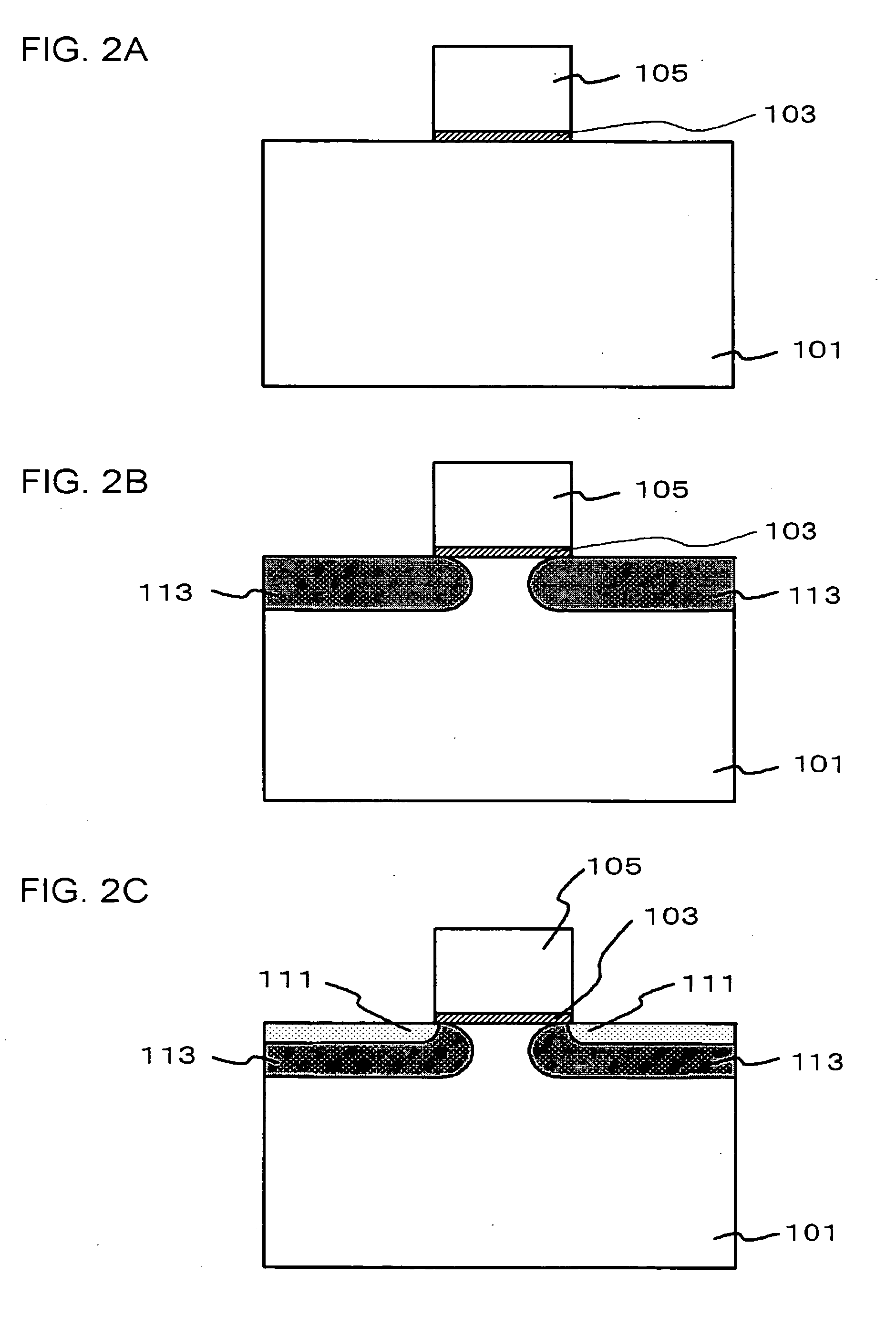
The manufacturing stability can be improved while effectively inhibiting the short-channel effect in the transistor according to the present invention. A halo impurity having a conductivity type opposite to a first conductivity type of a first impurity is ion-implanted into the silicon substrate 101, and thereafter the first impurity having the first conductivity type, is ion-implanted and then a flash lamp annealing is conducted to form a p-type halo region 113 and a n-type extension region 111. Then, the second impurity having the first conductivity type is ion-implanted into the silicon substrate 101, and then a flash lamp annealing is conducted to form a n-type source / drain region 109. Then, the impurity contained in the silicon substrate 101 is activated via spike RTA.

Description

[0001] This application is based on Japanese patent application NO. 2005-059554, the content of which is incorporated hereinto by reference. BACKGROUND OF THE INVENTION [0002] 1. Field of the Invention The present invention relates to a method for manufacturing a field effect transistor. [0003] 2. Description of the Related Art [0004] In order to achieve more rapid operation of a field effect transistor, technological developments such as providing a very short gate length of the field effect transistor, providing a shallow source / drain region and the like are proceeded. Such technologies includes a technology described in Japanese Patent Laid-Open No. 2004-253,446. [0005] Japanese Patent Laid-Open No. 2004-253,446 points out a fact that, in the process for manufacturing a metal oxide semiconductor (MOS) transistor, a redistribution is occurred as a diffusion of an implanted impurity is occurred during an annealing process after an ion implantation process, and therefore a dispersio...

Claims


Application Information

Patent Timeline
Patent Type & Authority Applications(United States)
IPC IPC(8): H01L21/336H01L21/425
CPCH01L21/26513H01L21/324H01L21/823807H01L21/823814H01L29/1083H01L21/2658
Inventor MINEJI, AKIRA
Owner RENESAS ELECTRONICS CORP
Learn More