

Method for manufacturing field effect transistor
a technology of field effect transistor and manufacturing method, which is applied in the direction of transistors, semiconductor devices, electrical appliances, etc., to achieve the effects of improving efficiency, enhancing diffusion of impurities, and improving use characteristics
- Summary
- Abstract
- Description
- Claims
- Application Information
AI Technical Summary
Benefits of technology
Problems solved by technology
Method used
Image

Examples
first embodiment
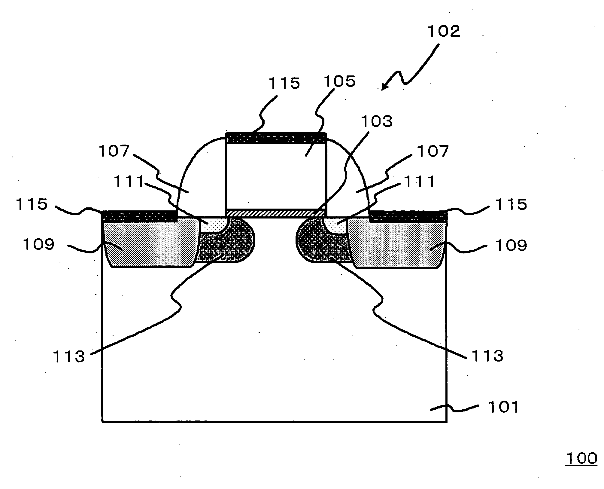
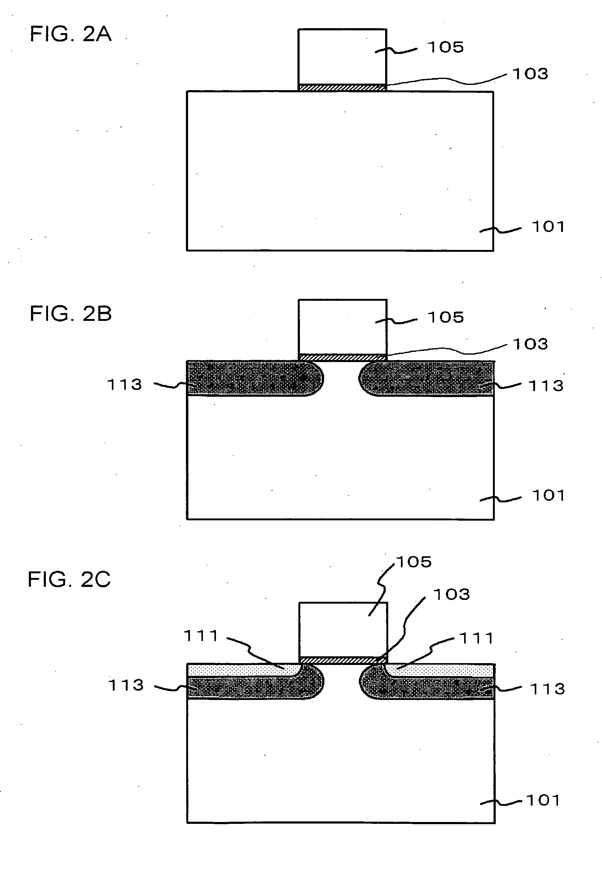
[0029]FIG. 1 is a cross-sectional view, schematically showing a configuration of a semiconductor device according to the present embodiment. A semiconductor device 100 shown in FIG. 1 comprises a n-type metal oxide semiconductor field effect transistor (MOSFET) 102. While it is not shown in FIG. 1, an element-separating region is provided in a peripheral portion of the n-type MOSFET 102.
[0030] In the n-type MOSFET 102, a pair of n-type source / drain regions 109 is provided in a silicon substrate 101 having p-type conductivity, and a channel region (not shown) is formed between the regions. The n-type source / drain region 109 is an impurity-diffusing region functioning as a source region or a drain region. A SiON film is provided on the channel region as a gate insulating film 103, and a polycrystalline silicon film that functions as a gate electrode 105 is formed on the SiON film so as to contacted therewith. Further, a side wall insulating film 107 that covers side walls of the gate...
second embodiment
[0065] While the example of the semiconductor device 100 having the n-type MOSFET 102 is described in the first embodiment, the a configuration of the present invention may also be applied to a complementary metal oxide semiconductor field effect transistor (CMOSFET).
[0066]FIG. 5 is a cross-sectional view, illustrating a configuration of a semiconductor device of the present embodiment. A semiconductor device 110 shown in FIG. 5 comprises a CMOSFET composed of the n-type MOSFET 102 shown in FIG. 1 and a p-type MOSFET 104.
[0067] The p-type MOSFET 104 is physically isolated and electrically insulated from the n-type MOSFET 102 by an element separating region 117. The p-type MOSFET 104 is formed in a n-type well 119 provided in the silicon substrate 101. The p-type MOSFET 104 also comprises a n-type halo region 125, a p-type extension region 123 and a p-type source / drain region 121, in place of the n-type source / drain region 109 of the n-type MOSFET 102, the n-type extension region 1...
example 1
[0085] A semiconductor device 100 comprising a p-type MOSFET 104 was manufactured via the procedure shown in FIG. 4. In step 103 and step 105, a laser beam was continuously irradiated. In this case, the highest available temperature was set to 1,400 degree C. Here, in this example and the following examples, the heating temperature during the formation of the side wall insulating film 107 was set to 700 degree C. In addition, in the spike RTA of step 106, a heating rate was set to 250 degree C. / sec., and highest available temperature for the surface of the silicon substrate 101 was set to 1,050 degree C.
PUM
 Abstract
Description
Claims
Application Information