Organic light-emitting devices with mixed electron transport materials

Inactive Publication Date: 2006-09-14
EASTMAN KODAK CO
19 Cites 126 Cited by

AI-Extracted Technical Summary

Problems solved by technology

While organic electroluminescent (EL) devices have been known for over two decades, their performance limitations have represented a barrier to many desirable applications.
However, the Bphen/Alq mix of Seo et al., shows inferior stability and falls outside the scope of the current invention.
However, these devices do not have the desire...

Method used

[0029] Embodiments of the invention may also exhibit high operational stability and give low voltage rises over the lifetime of the devices and can be produced with high reproducibility and consistently to provide good light efficiency.
[0096] The further layer as described in the invention contains a first compound, at least one second compound and a metal with a work function less than 4.2 eV. The first compound has the lowest LUMO value of the compounds in the layer. In addition, at least one second compound is a low voltage electron-transporting compound. The combination of both the first and second compounds with the metal in the further layer of the invention in the aforementioned ratios, give devices that have reduced drive voltages even lower when compared to the devices in which either the first or second compound are incorporated alone in said layer.
[0110] While not always necessary, it is often useful that a hole-injecting layer 130 be provided between anode 120 and hole-transporting layer 132. The hole-injecting material can serve to improve the film formation property of subsequent organic layers and to facilitate injection of holes into the hole-transporting layer. Suitable materials for use in the hole-injecting layer include, but are not limited to, porphyrinic compounds such as those described in U.S. Pat. No. 4,720,432, and plasma-deposited fluorocarbon polymers such as those described in U.S. Pat. No. 6,208,075. Alternative hole-injecting materials reportedly useful in organic EL devices are described in EP 0 891 121 A1 and EP 1 029 909 A1.
[0159] An important relationship for choosing a dye as a electroluminescent component is a comparison of the bandgap potential which is defined as the energy difference between the highest occupied molecular orbital and the lowest unoccupied molecular orbital of the molecule. For efficient energy transfer from the non-electroluminescent compound to the electroluminescent compound molecule, a necessary condition is that the band gap of the electroluminescent compound is smaller than that of the non-electroluminescent compound or compounds.
[0166] Z completes a heterocyclic nucleus containing at least two fused aromatic rings, at least one of which is an azole or azine ring. Additional rings, including both aliphatic and aromatic rings, can be fused with the two required rings, if required. To avoid adding molecular bulk without improving on function the number of ring atoms is usually maintained at 18 or less.
[0179] A preferred embodiment of the luminescent layer consists of a host material doped with fluorescent dyes. Using this method, highly efficient EL devices can be constructed. Simultaneously, the color of the EL devices can be tuned by using fluorescent dyes of different emission ...

Benefits of technology

[0020] The OLED device has a light-emitting layer (LEL) that exhibits good luminance efficiency and stabilit...

Abstract

An OLED device comprises a cathode, an anode, a light emitting layer, and on the cathode side of said emitting layer, a further layer containing a) a first compound that has the lowest LUMO value of the compounds in the layer, in an amount greater than or equal to 10% by volume and less than 100% by volume of the layer; b) at least one second compound exhibiting a higher LUMO value than the first compound, where at least one of the second compounds is a low voltage electron transport material, the total amount of such second compounds(s) is less than or equal to 90% by volume of the layer; and c) a metallic material based on a metal having a work function less than 4.2 eV.

Application Domain

Technology Topic

Image

  • Organic light-emitting devices with mixed electron transport materials
  • Organic light-emitting devices with mixed electron transport materials
  • Organic light-emitting devices with mixed electron transport materials

Examples

  • Experimental program(7)

Example

Example 1
LUMO Values
[0235] An important relationship exists when selecting the first compound(s) and second compound(s) of the invention. A comparison of the LUMO values of the first and second compounds in the layer of the invention, must be carefully considered. In devices of the invention, for there to be a drive voltage reduction over devices that contain only a first compound or only a second compound, there must be a difference in the LUMO values of the compounds. The first compound must have a lower LUMO value (more negative) than the second compound, or compounds (less negative).
[0236] The LUMO values are typically determined experimentally by electrochemical methods. A Model CHI660 electrochemical analyzer (CH Instruments, Inc., Austin, Tex.) was employed to carry out the electrochemical measurements. Cyclic voltammetry (CV) and Osteryoung square-wave voltammetry (SWV) were used to characterize the redox properties of the compounds of interest. A glassy carbon (GC) disk electrode (A=0.071 cm2) was used as working electrode. The GC electrode was polished with 0.05 um alumina slurry, followed by sonication cleaning in Milli-Q deionized water twice and rinsed with acetone in between water cleaning. The electrode was finally cleaned and activated by electrochemical treatment prior to use. A platinum wire served as counter electrode and a saturated calomel electrode (SCE) was used as a quasi-reference electrode to complete a standard 3-electrode electrochemical cell. Ferrocene (Fc) was used as an internal standard (EFC=0.50 V vs. SCE in 1:1 acetonitrile/toluene, 0.1 M TBAF). Mixture of acetonitrile and toluene (50%/50% v/v, or 1:1) was used as organic solvent system. The supporting electrolyte, tetrabutylammonium tetraflouroborate (TBAF) was recrystallized twice in isopropanol and dried under vacuum. All solvents used were low water grade (<20 ppm water). The testing solution was purged with high purity nitrogen gas for approximately 5 minutes to remove oxygen and a nitrogen blanket was kept on the top of the solution during the course of the experiments. All measurements were performed at ambient temperature of 25±1° C. The oxidation and reduction potentials were determined either by averaging the anodic peak potential (Ep,a) and cathodic peak potential (Ep,c) for reversible or quasi-reversible electrode processes or on the basis of peak potentials (in SWV) for irreversible processes. All LUMO values pertaining to this application are calculated from the following:
Formal reduction potentials vs. SCE for reversible or quasi-reversible processes;
EO′red=(Epa+Epc)/2
Formal reduction potentials vs. Fc;
EO′red vs. Fc=(EO′red vs. SCE)−EFC
where EFc is the oxidation potential Eox, of ferrocene; Estimated lower limit for LUMO;
LUMO═HOMOFc−(EO′red vs. Fc)
where HOMOFc (Highest Occupied Molecular Orbital for ferrocene)=−4.8 eV.
[0237] The LUMO values for some first and second compounds are listed in Table 1. To make a selection of compounds useful in the invention, the first compound should have a lower LUMO value than its paired second compound(s). TABLE 1 LUMO Values for Representative Materials Material LUMO (eV) A-7/B-1 −2.50 A-8/B-2 −2.50 A-10 −2.44 A-11 −2.45 A-12 −2.40 A-13 −2.77 A-14 −2.83 A-15 −3.02 A-16 −2.72 A-17 −3.24 A-18 −2.52 A-19 −2.83 A-22 −2.35 B-4 −2.4 B-5 −2.3 B-6 −2.3

Example

Example 2
Synthesis—Scheme 1
[0238]
Example 2
Synthesis—Method
[0239] Preparation of compound (3): Under a nitrogen atmosphere, acetylenic compound (2) (2.0 g, 12 mMole), was dissolved in dimethylformamide (DMF) (100 mL) and the solution cool to 0° C. Potassium t-butoxide (KButO) (1.4 g, 12 mMole), was added and the mixture stirred well for approximately 15 minutes. To this mixture was then added the benzophenone (1) (3.53 g, 30 mMole). Stirring was continued at 0° C. for approximately 30 minutes and then allowed to come to room temperature over a 1-hour period. At the end of this time the solution was cooled to 0° C. and the reaction treated with saturated sodium chloride (20 mL). The mixture was then diluted with ethyl acetate, washed with 2N—HCl (×3), dried over MgSO4, filtered and concentrated under reduced pressure. The crude product was triturated with petroleum ether to give the product as an off-white solid. Yield of compound (3), 3.0 g.
[0240] Preparation of Compound, A-16: Compound (3) (7.0 g, 15 mMole) was dissolved in methylene chloride (CH2Cl2) (70 mL), and stirred at 0° C. under a nitrogen atmosphere. To this solution was added triethylamine (NEt3) (1.56 g, 15 mMole) and then treated drop by drop with methanesulfonyl chloride (CH3SO2Cl) (1.92 g, 15 mMole), keeping the temperature of the reaction in the range 0-5° C. After the addition the solution was stirred at 0° C. for 30 minutes and then allowed to warm to room temperature over 1 hour. The reaction was then heated to reflux, distilling off the methylene chloride solvent and gradually replacing it with xylenes (a total of 70 mL). When the internal temperature of the reaction reached 80° C., collidine (2.40 g, 19.82 mMole), dissolved in xylenes (10 mL) was added drop by drop over a 10-minute period. The temperature was then raised to 110° C. and held at this temperature for 4 hours. After this period the reaction was cooled and concentrated under reduced pressure. The oily residue was stirred with methanol (70 mL) to give the crude product. This material was filtered off, washed with methanol and petroleum ether to give inventive compound A-16 as a bright red solid. Yield 1.5 g with a melting point of 300-305° C. The product may be further purified by sublimation (250° C. @ 200 millitorr) with a N2 carrier gas.

Example

Example 3
EL Device Fabrication
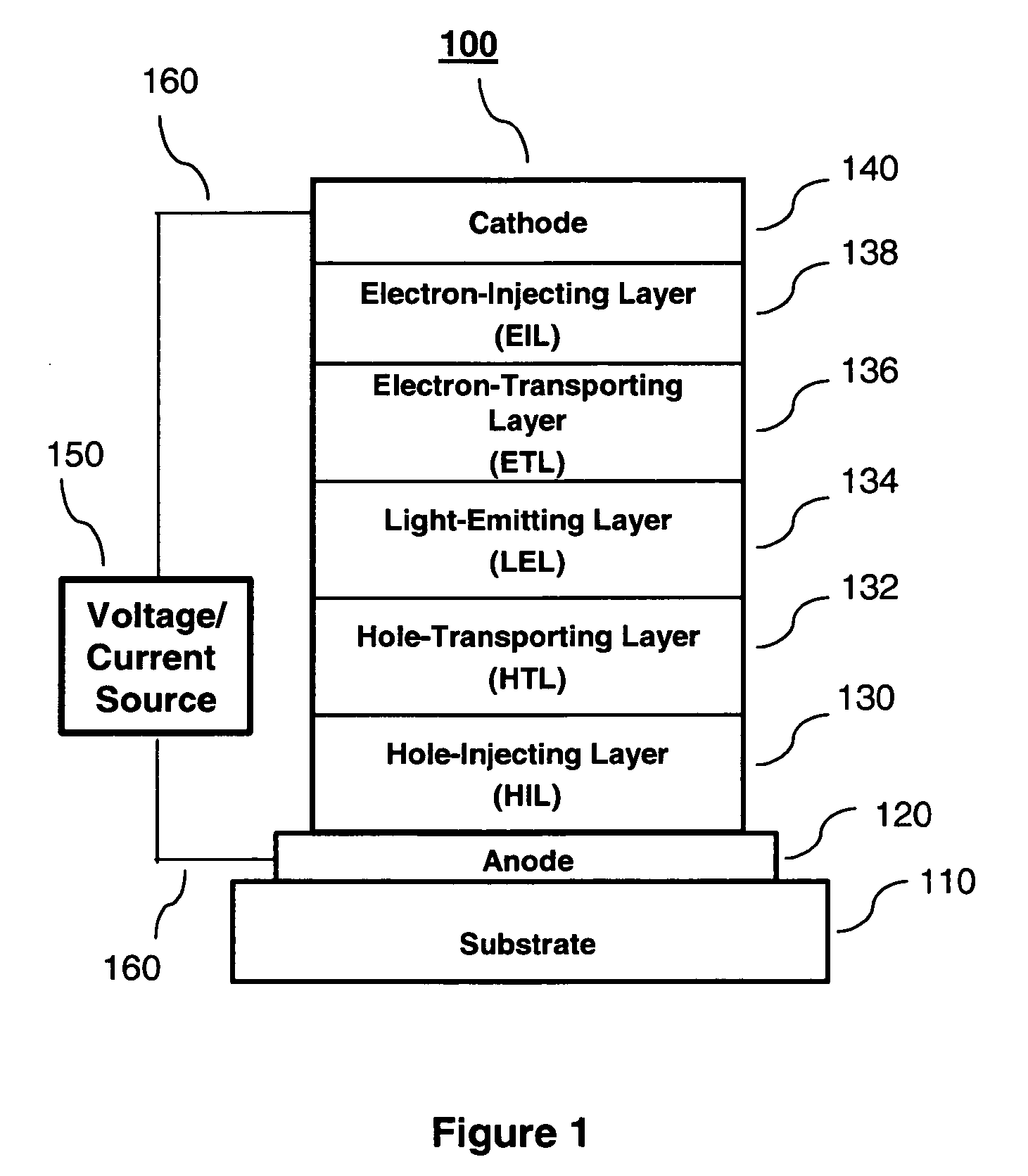
[0241] EL devices satisfying the requirements of the invention and for the purposes of comparison, were constructed in the following manner:
[0242] A glass substrate coated with an 85 nm layer of indium-tin oxide (ITO) as the anode was sequentially ultrasonicated in a commercial detergent, rinsed in deionized water, degreased in toluene vapor and exposed to oxygen plasma for about 1 min.
[0243] a) Over the ITO was deposited a 1 nm fluorocarbon (CFx) hole-injecting layer (HIL) by plasma-assisted deposition of CHF3.
[0244] b) A hole-transporting layer (HTL) of N,N′-di-1-naphthalenyl-N,N′-diphenyl-4,4′-diaminobiphenyl (NPB) having a thickness of 75 nm was then evaporated onto a).
[0245] c) A 35 nm light-emitting layer (LEL) of tris(8-quinolinolato)aluminum (III) (Alq) was then deposited onto the hole-transporting layer.
[0246] d) A 35 nm electron-transporting layer (ETL) of the materials and amounts indicated in Tables 2-7 and 9 were then deposited onto the light-emitting layer.
[0247] e) On top of the ETL was deposited a 0.5 nm layer of LiF.
[0248] f) On top of the LiF layer was deposited a 130 nm layer of Al to form the cathode.
[0249] The above sequence completed the deposition of the EL device. The device was then hermetically packaged in a dry glove box for protection

PUM

PropertyMeasurementUnit
Fraction0.001fraction
Fraction0.1fraction
Fraction0.01fraction
tensileMPa
Particle sizePa
strength10

Description & Claims & Application Information

We can also present the details of the Description, Claims and Application information to help users get a comprehensive understanding of the technical details of the patent, such as background art, summary of invention, brief description of drawings, description of embodiments, and other original content. On the other hand, users can also determine the specific scope of protection of the technology through the list of claims; as well as understand the changes in the life cycle of the technology with the presentation of the patent timeline. Login to view more.

Similar technology patents

Classification and recommendation of technical efficacy words

Why Eureka
Try Eureka