
High efficiency inorganic nanorod-enhanced photovoltaic devices

a photovoltaic device and nanorod technology, applied in the field of photovoltaic devices comprising nanostructured materials, can solve the problems of limiting the conversion efficiency of a standard cell to about 44%, and none is efficient enough to drive down the cost involved in the production and use of this technology

Inactive Publication Date: 2006-09-21
GENERAL ELECTRIC CO
View PDF13 Cites 362 Cited by
  • Summary
  • Abstract
  • Description
  • Claims
  • Application Information

AI Technical Summary

Benefits of technology

[0014] In some embodiments, the devices of the present invention are used as sources of power in residential and commercial infrastructures. In some or other embodiments, these devices are used as power supplies in portable equipment. In other embodiments, satellite power panels utilize this technology to reduce size and weight, and increase reliability, of space-deployed electrical photovoltaic panels.

Problems solved by technology

Single and multi-junction p-n solar cells are used for this purpose, but none are efficient enough to drive down the costs involved in the production and use of this technology.
Consequently, competition from conventional sources of electricity precludes the widespread use of such solar cell technology.
This loss alone limits the conversion efficiency of a standard cell to about 44%.
Additionally, recombination of such photo-excited electron-hole pairs reduces the efficiency further.
Although this latter reduction in efficiency can be overcome by using other materials with appropriate properties, particularly long diffusion lengths of the photo-generated carriers, this still does not bring this technology to a cost parity with more conventional sources of electricity.
Recent developments in multi-junction technologies are costly and not enough to justify a shift to photovoltaic (PV) technology in homes or industries.
Additionally, the incorporation of nanostructures into such devices has thus far failed to achieve efficiencies sufficient to make such solar power technologies economically viable.
Such arrays, however, were not configured for use in photovoltaic devices, nor was it suggested how such arrays might serve to increase the efficiency of solar cells.
However, such nanowires are not active PV elements; they merely serve in an anti-reflective capacity.

Method used


Image

  • High efficiency inorganic nanorod-enhanced photovoltaic devices
  • High efficiency inorganic nanorod-enhanced photovoltaic devices
  • High efficiency inorganic nanorod-enhanced photovoltaic devices

Examples


example 1

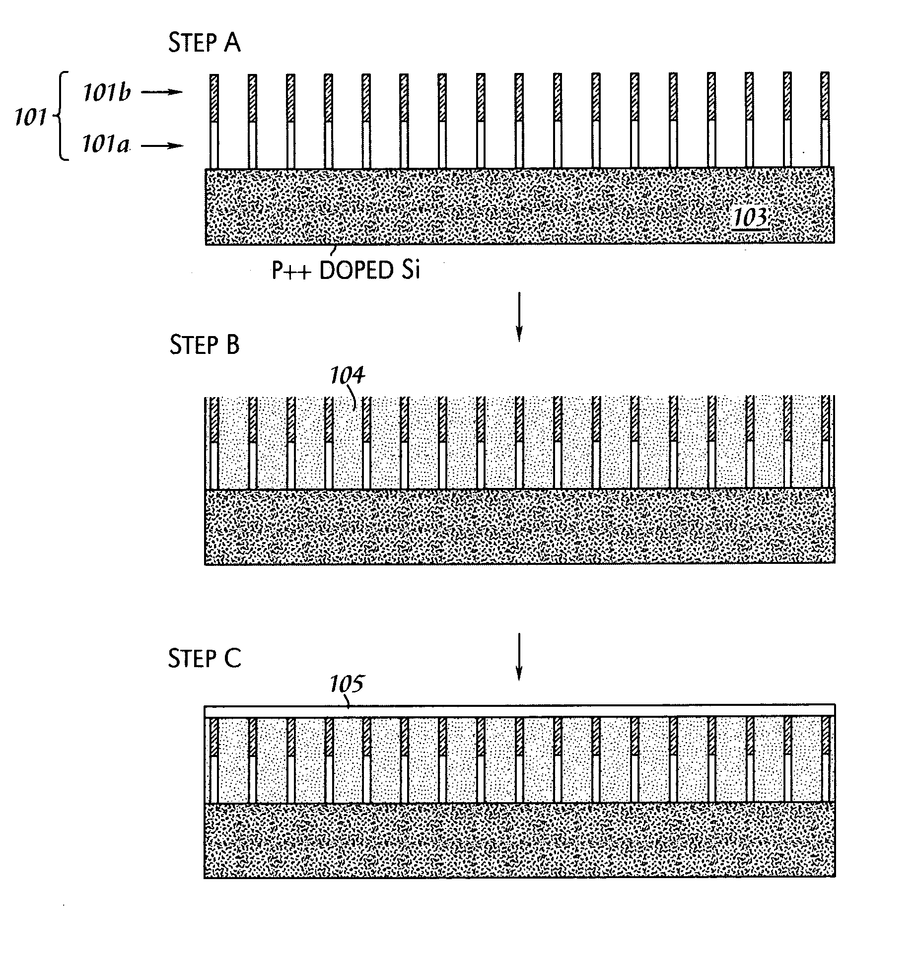
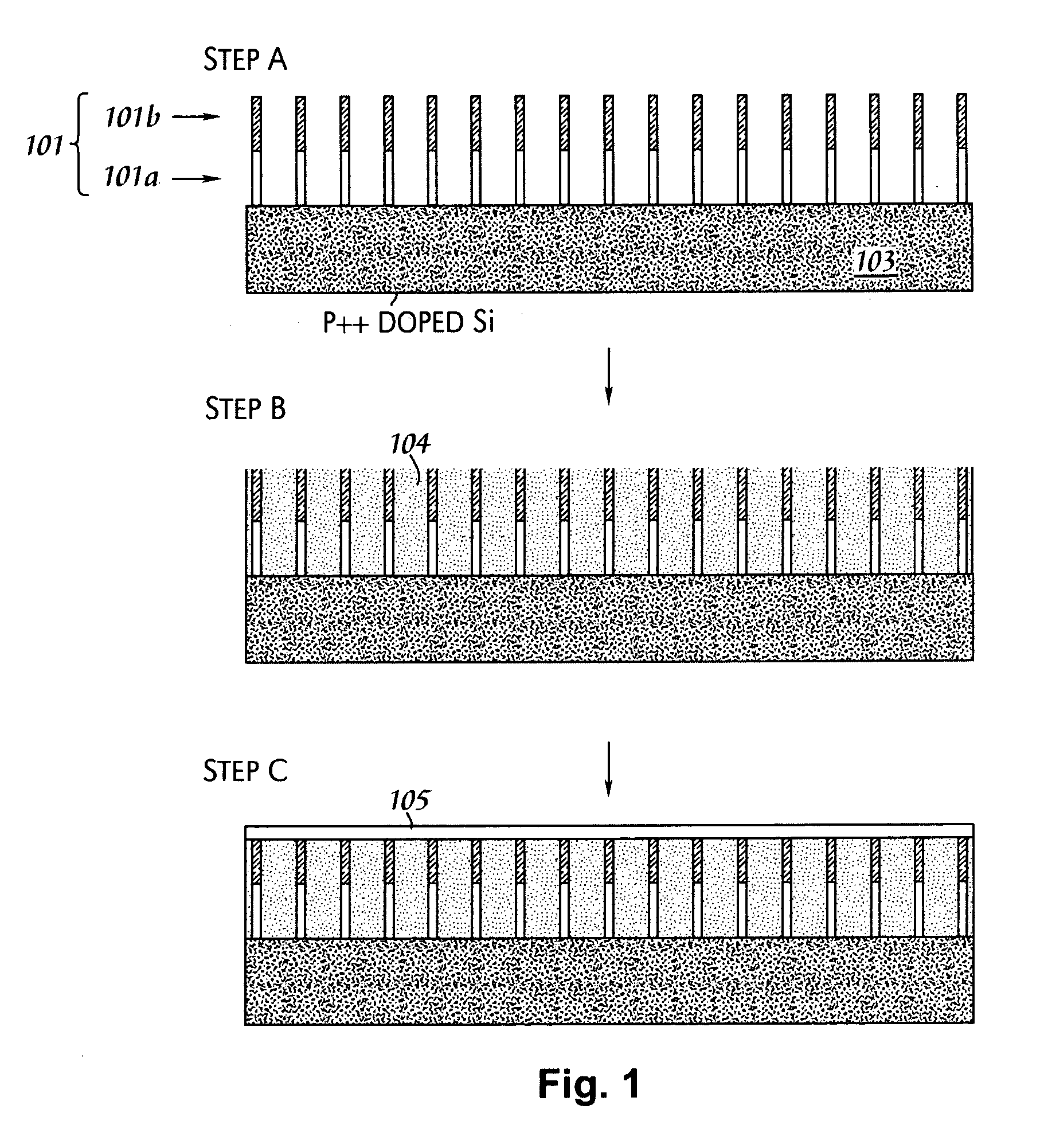
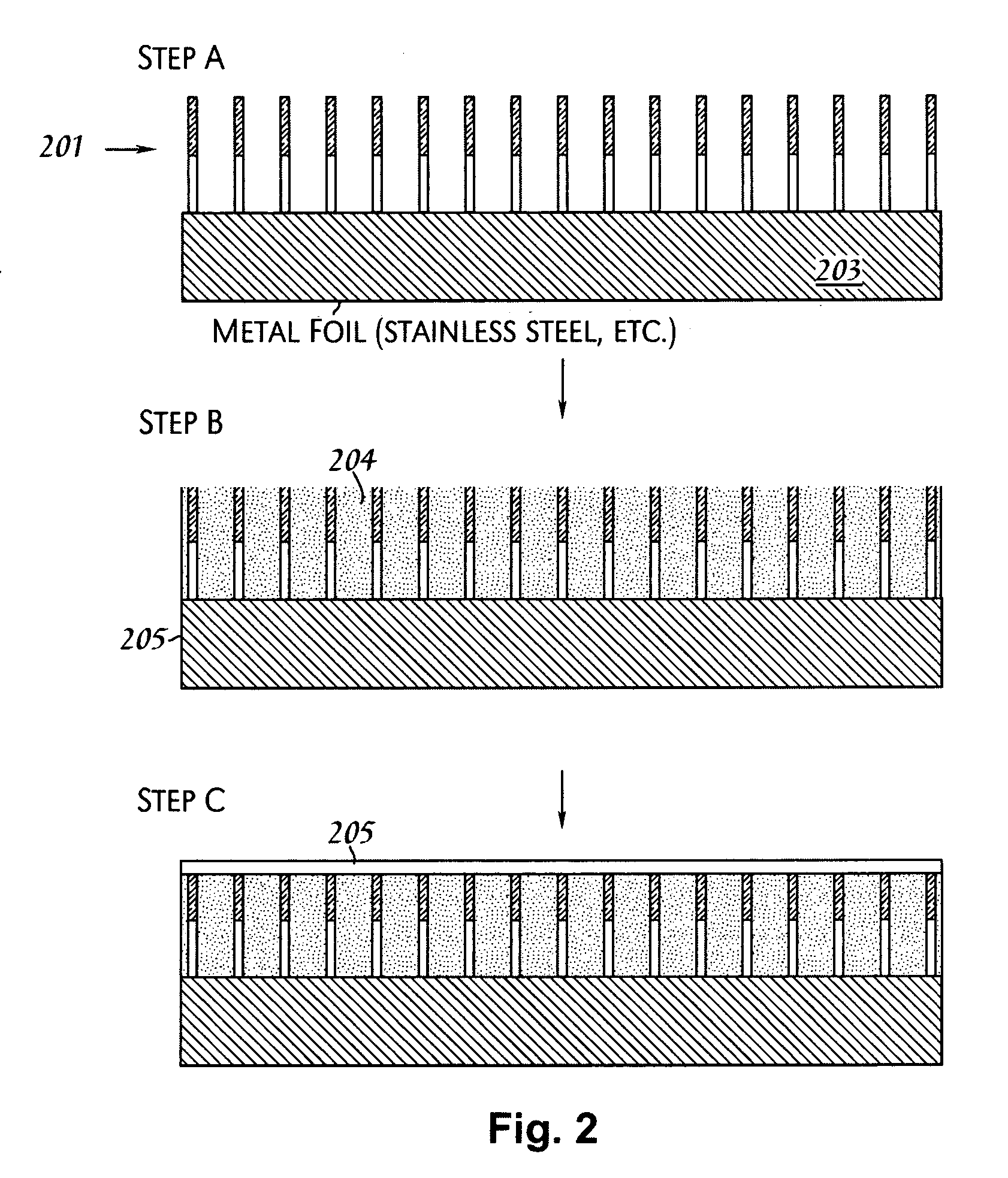
[0101] This example illustrates an embodiment where wet etching is used to produce nanowire arrays for use in PV devices of the present invention.

[0102] Wet etching of bulk or thin film substrates to produce nanowire arrays may be achieved as follows. A bulk Si substrate is cleaned using known procedures. The substrate is then place in a solution comprising 1 M AgNO3 in HF. The temperature of the bath may be room temperature or as high as 80° C. This process leads to the precipitation of nanoscale Ag dendrite particles on the surface. The nanoscale particles allow for directional electric fields perpendicular to the surface of the substrate to form that are concentrated at the nanoscale. This permits a galvanic process to occur at this length scale. An illustrative example of a nanowire array formed by wet etching on Si wafers is shown in the scanning electron micrograph (SEM) of FIG. 13. Nanowire arrays on Si substrates are formed at an angle of 45 degrees to the substrate surfa...

example 2

[0104] This example illustrates CVD growth of aligned nanowire arrays for use in PV devices of the present invention.

[0105] Aligned nanowire arrays may be grown by CVD by first cleaning the substrate using known procedures. In the case of growth on Si, the substrate is also etched in HF to remove the native oxide. The substrate is then immediately placed inside the deposition system (evaporation or sputtering) that will place a thin metal catalyst layer onto the surface. The catalyst may also be deposited from solution by spin coating. The typical thickness of the catalyst layer is 1-30 nm. The metal-coated substrate is then place in a horizontal low pressure CVD (LPCVD) furnace and heated to between 400-700° C. Once the set temperature is attained, hydrogen and silane flow at rates of between 1 and 300 sccm for 5-60 minutes. FIG. 17 is an SEM image depicting an example of such a CVD-produced Si nanowire array grown at 560° C. FIG. 25 is an SEM image depicting an example of CVD-pro...

example 3

[0106] This example illustrates the fabrication of a solar cell device in accordance with an embodiment of the present invention.

[0107] A p-type silicon substrate comprising a thin region of phosphorus (by ion implantation or diffusion) to form a thin n-type region on the top surface of the substrate is coated with silicon nitride on both sides. The p-n junction is located 0.5-2 microns below the surface. The top nitride layer is removed by reactive ion etching. The substrate is then wet etched in AgNO3 / HF to form a nanowire array on the top surface. The silicon nitride on the back side is then removed by reactive ion etching and metal (Al) is deposited on the backside. The wafer is then annealed at 400° C. in a hydrogen atmosphere. A TCO such as ITO is then deposited onto the top nanowire surface and metal patterns are deposited on the ITO through a shadow mask. FIG. 18 is an SEM image depicting such a solar cell in cross section.


PUM

PropertyMeasurementUnit
angleaaaaaaaaaa
angleaaaaaaaaaa
diameteraaaaaaaaaa

Abstract

The present invention is directed to photovoltaic devices comprising nanostructured materials, wherein such photovoltaic devices are comprised exclusively of inorganic components. Depending on the embodiment, such nanostructured materials are either 1-dimensional nanostructures or branched nanostructures, wherein such nanostructures are used to enhance the efficiency of the photovoltaic device, particularly for solar cell applications. Additionally, the present invention is also directed at methods of making and using such devices.

Description

TECHNICAL FIELD [0001] The present invention relates generally to photovoltaic devices, and specifically to photovoltaic devices comprising nanostructured materials. BACKGROUND INFORMATION [0002] Presently, silicon (Si) is the most commonly used material in the fabrication of solar cells, such solar cells being used for converting sunlight into electricity. Single and multi-junction p-n solar cells are used for this purpose, but none are efficient enough to drive down the costs involved in the production and use of this technology. Consequently, competition from conventional sources of electricity precludes the widespread use of such solar cell technology. [0003] The primary loss process in existing solar cells occurs when a photo-excited electron-hole pair quickly looses any energy it may have in excess of the bandgap. This loss alone limits the conversion efficiency of a standard cell to about 44%. Additionally, recombination of such photo-excited electron-hole pairs reduces the e...

Claims


Application Information

Patent Timeline
Patent Type & Authority Applications(United States)
IPC IPC(8): H01L31/00
CPCB82Y20/00H01L31/035245H01L31/18H01L31/035227H01L31/1085
Inventor TSAKALAKOS, LOUCASLEE, JI-UNGKORMAN, CHARLES STEVENLEBOEUF, STEVEN FRANCISEBONG, ABASIFREKEWOJNAROWSKI, ROBERTSRIVASTAVA, ALOK MANISULIMA, OLEG
Owner GENERAL ELECTRIC CO
Learn More