Nonvolatile nanochannel memory device using organic-inorganic complex mesoporous material

Inactive Publication Date: 2006-09-21
SAMSUNG ELECTRONICS CO LTD
View PDF12 Cites 30 Cited by
  • Summary
  • Abstract
  • Description
  • Claims
  • Application Information

AI Technical Summary

Benefits of technology

[0015] Accordingly, embodiments of the present invention have been made keeping in mind the above problems occurring in the related art, and an object of embodiments of the present invention is to provide a memory device, which ensures regular charge transfer paths

Problems solved by technology

Although almost all conventional nonvolatile memory devices are manufactured using standard silicon technology, the silicon-based device thus manufactured has shortcomings, such as a complicated structure and a large-sized single memory cell, so that high memory capacity is difficult to realize.
Manufacturing silicon-based memory having a high memory capacity with high integration requires a fining process, capable of decreasing line and space widths per unit area which results in high costs of manufacturing memory chips.
Moreover, current manufacturing techniques of the chips do not allow them to be further miniaturized, and hence, profitability problems are now being faced.
However, the above memory device can be manufactured only by thermal deposition using an expensive evaporator, instead of a simple process such as spin coating, due to the use of a monomer as a raw material, and hence, has no advantage in terms of processability.
Although the conducting polymer may be used for spin coating, its molecular weight and distribution are difficult to accurately control.
Thus, reproducibility of the material is problematic, and uniform performance of the device cannot be realized.
However, the fluorine-based polymer is difficult to apply due to hydrophobic properties

Method used


Image

  • Nonvolatile nanochannel memory device using organic-inorganic complex mesoporous material
  • Nonvolatile nanochannel memory device using organic-inorganic complex mesoporous material
  • Nonvolatile nanochannel memory device using organic-inorganic complex mesoporous material

Examples


example 1

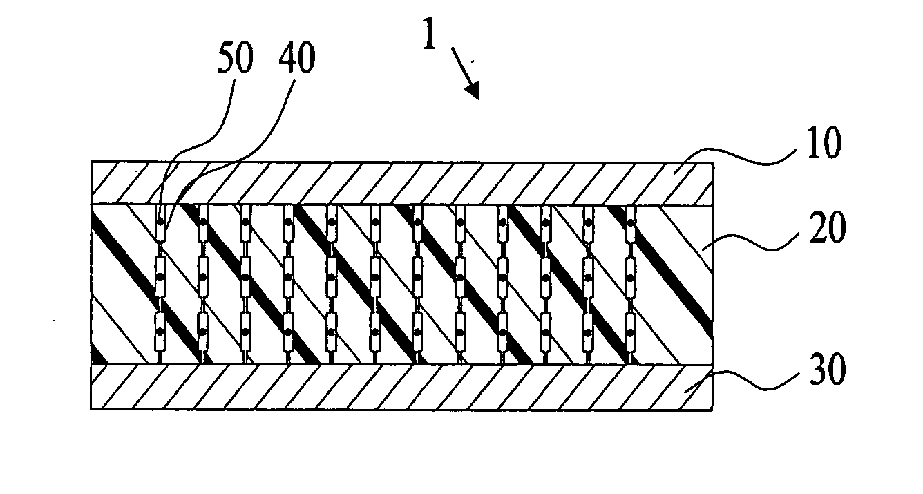
[0088] A memory device was manufactured as follows. First, Al serving as a lower electrode was deposited to a thickness of 80 nm on a glass substrate having a size of 50×50 mm2 using thermal deposition.

[0089] Then, an organic-inorganic complex matrix precursor for use in manufacturing an organic-inorganic complex thin film having nanopores was manufactured according to the following procedures. That is, into a flask, 41.6 mmol (10.00 g) 2,4,6,8-tetramethyl-2,4,6,8-cyclotetrasiloxane was loaded, and then diluted with 100 ml of tetrahydrofuran (THF), and added with 700 mg of 10 wt % Pd / C (palladium on charcoal). Subsequently, 177.8 mmol (3.20 ml) distilled water was added, and the generated hydrogen gas was removed. The reaction was conducted at room temperature for 5 hr, after which the reaction solution was filtered through a celite and MgSO4. The filtrate was placed under a reduced pressure of about 0.1 torr to remove volatile material, and 41.6 mmol (12.6 g) compound thus obtaine...

example 2

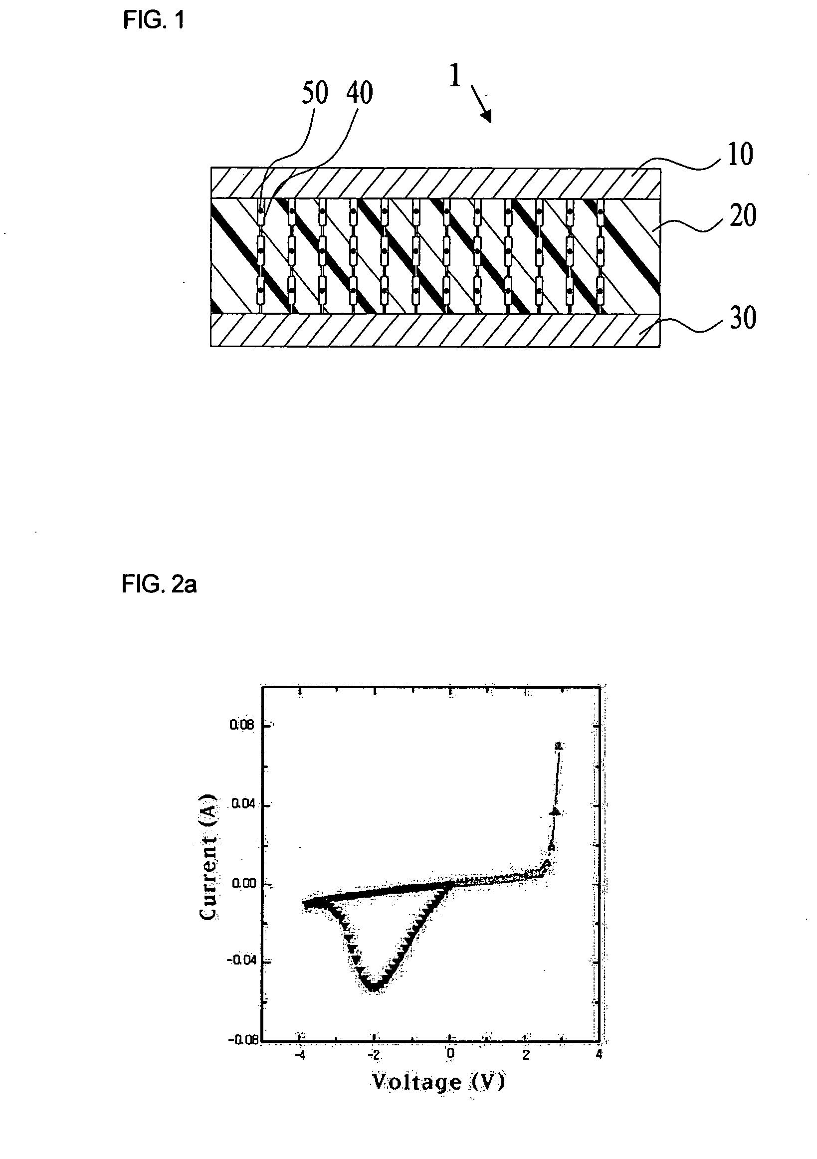
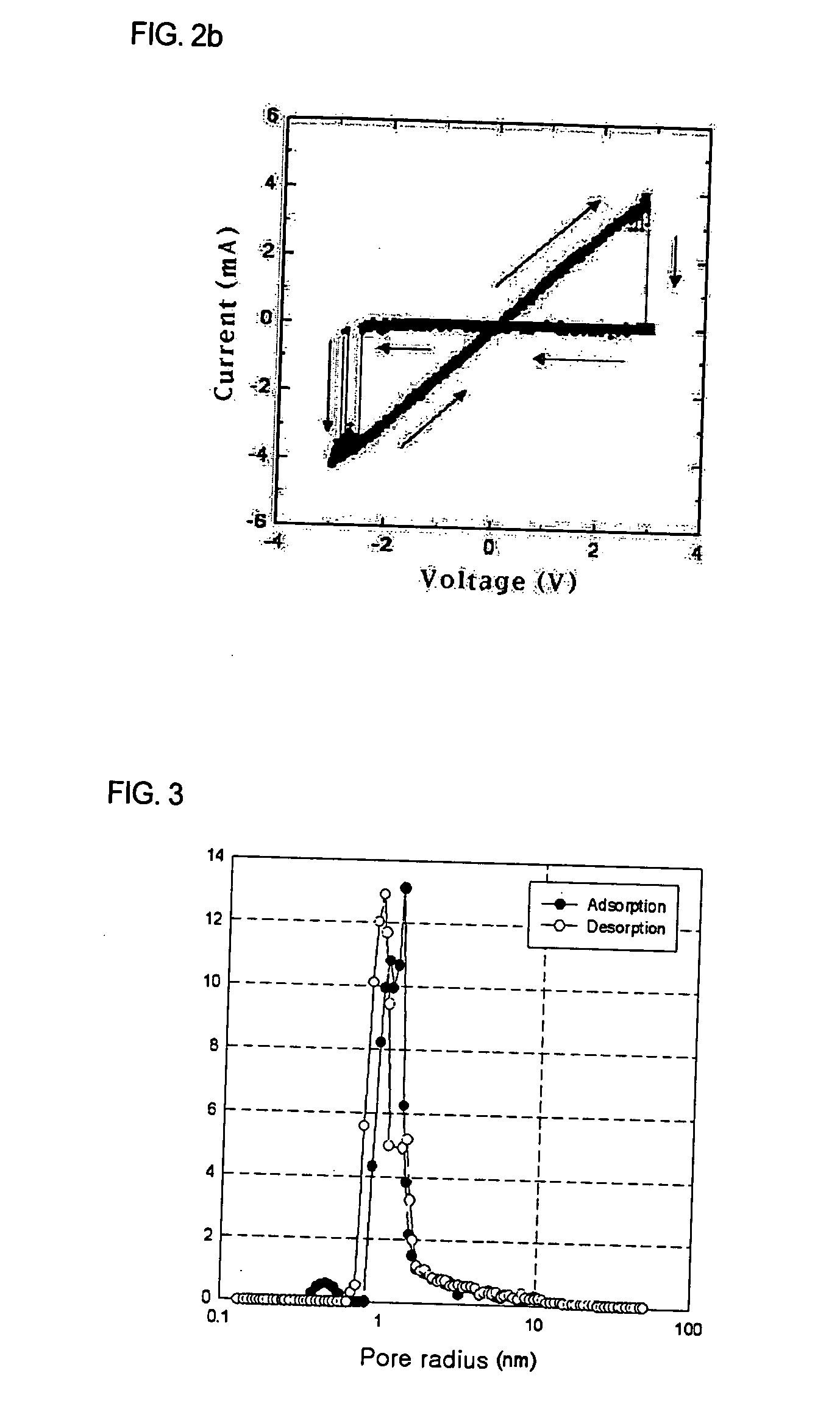
[0095] A memory device was manufactured in the same manner as in Example 1, with the exception that an upper electrode was formed of Au. The I-V graph showing memory properties of the device is shown in FIG. 5. As confirmed in the I-V graph, when the upper electrode was formed of Au, fast switching occurred. That is, low resistance was switched to high resistance at +2 V, resulting in a reset state. On the other hand, high resistance was switched to low resistance at −1.5 V, exhibiting a set state. The resistance values of two states were measured at 453Ω and 230Ω, respectively. The two different resistance states may be read even at a low reading voltage, and thus, the device may be used as a memory device.

[0096] As described hereinbefore, embodiments of the present invention provide a nonvolatile nanochannel memory device using an organic-inorganic complex mesoporous material. A memory device using a mesoporous material of embodiments of the present invention has nonvolatile prop...


PUM

PropertyMeasurementUnit
Temperatureaaaaaaaaaa
Thicknessaaaaaaaaaa
Thicknessaaaaaaaaaa

Abstract

A memory device of the current invention includes a memory layer having nanochannels sandwiched between an upper electrode and a lower electrode, in which the memory layer is made of an organic-inorganic complex for use in formation of nanopores, and has metal nanoparticles or metal ions fed into the nanopores. Therefore, the memory device has excellent processability, high reproducibility, and uniform performance.

Description

CROSS-REFERENCE TO RELATED PATENT APPLICATION [0001] This application claims the benefit of Korean Patent Application No. 10-2005-22220, filed on Mar. 17, 2005, in the Korean Intellectual Property Office, the disclosure of which is incorporated herein in its entirety by reference. BACKGROUND OF THE INVENTION [0002] 1. Field of the Invention [0003] Embodiments of the present invention relate, generally, to a nonvolatile nanochannel memory device using an organic-inorganic complex mesoporous material, and, more particularly, to a memory device, comprising a memory layer having nanochannels sandwiched between an upper electrode and a lower electrode, in which the memory layer is made of an organic-inorganic complex for use in formation of nanopores and having metal nanoparticles or metal ions fed into the nanopores. [0004] 2. Description of the Related Art [0005] Recently, with the rapid development of the information and communication industries, the demand for various memory devices ...

Claims


Application Information

Patent Timeline
IPC IPC(8): H01L23/58H01L21/4757
CPCB82Y10/00G11C13/0014G11C13/0016G11C2213/15H01L45/04H01L45/085H01L45/1233H01L45/1266H01L45/14H01L51/0036H01L51/0591H10N70/245H10N70/8416H10N70/20H10N70/881H10N70/826H10K85/113H10K10/50
Inventor LEE, KWANG HEEJOO, WON JAEYIM, JIN HEONGKANG, YOON SOK
Owner SAMSUNG ELECTRONICS CO LTD
Why Eureka
Try Eureka