Method for manufacturing semiconductor apparatus, and semiconductor apparatus and electric appliance

a manufacturing method and technology for semiconductors, applied in chemistry apparatus and processes, polycrystalline material growth, crystal growth process, etc., can solve the problems of increasing the thickness of the chip mounted on the csp, increasing the cost, and increasing the cost of manufacturing, so as to reduce the cost, increase the throughput, and reduce the thickness

Active Publication Date: 2006-10-05
SEMICON ENERGY LAB CO LTD
View PDF53 Cites 50 Cited by
  • Summary
  • Abstract
  • Description
  • Claims
  • Application Information

AI Technical Summary

Benefits of technology

[0011] In view of the foregoing, it is an object of the present invention to provide a package and a method for manufacturing the package by which chips can be reduced its thickness drastically without back grind that causes cracks and polishing marks; chips can be manufactured at lower cost with higher throughput; and the variations of thickness of chips can be prevented. Another object of the present invention is to provide electric appliances installed with the package.

Problems solved by technology

Therefore a chip having larger circuit size and larger amount of memory are necessary to be mounted on the limited capacity of the portable electric appliance.
For realizing further downsizing and weight saving of CSP, thinning of the chip mounted on CSP is becoming considered as a problem.
There are some cases that a crack is generated in addition to the polishing mark.
Both of the polishing mark and the crack cause chip destruction during a subsequent process.
The problem becomes serious as the thickness of a chip is reduced.
The stress relief is effective for making the polishing mark disappear with a depth of approximately several ten nm, however it is ineffective for making cracks disappear with a depth from several to 20 μm.
In addition, it becomes unfavorable that stress relief is carried out so as to make the cracks disappear since processing time becomes prolonged and the throughput in the process for manufacturing chips becomes decreased.
Since the thickness of a silicon wafer has an effect on the characteristics of a chip that is to be manufactured, there will arise a problem of variations of the characteristics due to such uneven thickness.
In addition, the unit cost of a silicon wafer is higher than that of a glass substrate or the like.
Although more than 12 inches sized silicon wafers are also on the market, the unit cost becomes further increased as increasing its size so that such silicon wafers are not suitable to provide low cost chip.
However, the silicon wafer with 12 inches in diameter is not suitable for mass-production since the number of chip manufactured from one silicon wafer is limited and throughput of the silicon wafer with only 12 inches is difficult to be improved.

Method used


Image

  • Method for manufacturing semiconductor apparatus, and semiconductor apparatus and electric appliance
  • Method for manufacturing semiconductor apparatus, and semiconductor apparatus and electric appliance
  • Method for manufacturing semiconductor apparatus, and semiconductor apparatus and electric appliance

Examples


embodiment mode 1

[0070] A method for packaging using a thin semiconductor film crystallized with a first and a second laser light will be explained in Embodiment Mode 1. In this embodiment mode, two TFTs exemplified as a semiconductor device, but not exclusively, a semiconductor device included in chips includes various circuit devices in the present invention. For example, a memory device, a diode, a photoelectric conversion device, a resistive element, a coil, a capacitance element, an inductor, or the like can be typically given, in addition to TFTs.

[0071] As shown in FIG. 5A, a metal film 501 is deposited over a first substrate 500 by sputtering. Here, tungsten is used for forming the metal film 501 and formed to have a thickness of from 10 to 200 nm, preferably, from 50 to 75 nm. In this embodiment mode, the metal film 501 is deposited directly on the first substrate 500, but the metal film 501 may also be deposited after covering the first substrate 500 by an insulating film such as silicon o...

embodiment mode 2

[0113] The structure of the laser irradiation device used for manufacturing a package according to the present invention will be described with reference to FIG. 4A and FIG. 4B.

[0114] Reference numeral 201 denotes a pulsed laser oscillator, Nd: YLF laser achieving power of 6W is used in the present invention. The laser oscillator 201 is converted into a second harmonic at an oscillation mode of TEM00 by a nonlinear optical device. The second harmonic is, not exclusively but preferably, used in this embodiment mode since the second harmonic is favorable in energy efficiency compared with higher harmonics. Its pulse frequency is 1 kHz, and pulse width is approximately 60 ns. A solid state laser achieving approximately output powers of 6 W is used in this embodiment mode, but a large laser that is capable of output powers of 300 W, for example, an XeCl excimer layer, or the like can also be used.

[0115] As a linear optical device, crystals such as KTP (KTiOPO4), BBO (β-BaB2O4), LBO (L...

embodiment mode 3

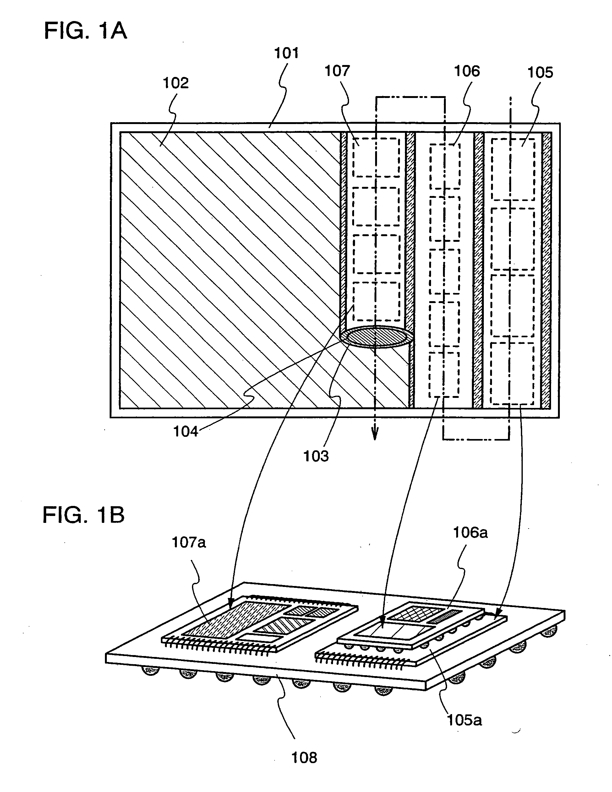
[0134] In case of manufacturing simultaneously a plurality of chips over a first substrate, it is necessary that chips are separated from each other by dicing prior to completing a package. The timing of the dicing will be explained in this embodiment mode.

[0135]FIG. 8 shows an example of a flaw chart for showing a manufacturing process of a package. The positions of pads, which serves as a terminal for electric interconnections to an integrated circuit, in wire bonding and in flip chip are different. In FIG. 8, the sequence of a flaw chart by which a pad is formed after forming a device is represented by a full line, and the sequence of a flaw chart by which a pad is formed before forming a device is represented by a dotted line.

[0136] The case that a pad is formed after forming a device will be explained hereinafter. First, a metal film is formed over a first substrate, and the surface of the metal film is oxidized, and then, a metal oxide film is formed. Second, an insulating f...


PUM

PropertyMeasurementUnit
thicknessaaaaaaaaaa
depthaaaaaaaaaa
depthaaaaaaaaaa

Abstract

According to the package and the method for manufacturing the package of the present invention, a chip can be formed extremely to be thin, and manufactured at lower cost and higher throughput, and the variations of a chip thickness can be reduced without back grind that causes cracks or polishing marks. In the present invention, a semiconductor film with a thickness of at most 500 μm deposited over a substrate serving as a support medium is crystallized with a CW laser light, and a chip having a semiconductor device is formed to have a total thickness of 5 μm, preferably at most 2 μm by using the crystallized semiconductor film. Consequently, the chip is mounted on an interposer after separating a substrate.

Description

BACKGROUND OF THE INVENTION [0001] 1. Field of the Invention [0002] The present invention relates to a semiconductor apparatus (package) and a method for manufacturing the semiconductor apparatus such as CSP (Chip size package) or MCP (Multi chip package) with an integrated circuit (IC) mounted. More specifically, the present invention relates to an electric appliance installed with the package. [0003] 2. Related Art [0004] A portable electric appliance as typified by a cellular phone or an electronic book is required various functions such as sending and receiving e-mails, speech recognition, image capturing using a small camera, and the like. On the other hand, downsizing and weight saving of the portable electric appliances needs from users are still increased. Therefore a chip having larger circuit size and larger amount of memory are necessary to be mounted on the limited capacity of the portable electric appliance. [0005] CSP (Chip size package), which is one type of packaging...

Claims


Application Information

Patent Timeline
Patent Type & Authority Applications(United States)
IPC IPC(8): H01L23/02H01L23/12C30B13/24C30B29/06H01L21/00H01L21/20H01L21/428H01L21/60H01L21/68H01L21/98H01L25/065H01L25/10
CPCC30B13/24C30B29/06H01L21/2026H01L21/6835H01L24/32H01L24/81H01L25/0657H01L25/105H01L25/50H01L2221/68354H01L2221/68359H01L2221/68363H01L2221/68368H01L2223/54473H01L2224/1134H01L2224/16145H01L2224/16225H01L2224/29198H01L2224/32145H01L2224/32225H01L2224/48091H01L2224/48227H01L2224/48465H01L2224/73265H01L2224/81203H01L2224/81205H01L2224/81801H01L2224/83102H01L2224/83192H01L2224/92125H01L2224/92247H01L2225/06524H01L2225/06555H01L2924/01004H01L2924/01013H01L2924/01029H01L2924/01032H01L2924/01033H01L2924/01046H01L2924/01047H01L2924/0105H01L2924/01056H01L2924/0106H01L2924/01078H01L2924/01079H01L2924/01082H01L2924/09701H01L2924/15311H01L2924/15331H01L2924/19041H01L2924/30105H01L2924/3025H01L2924/00013H01L2924/01005H01L2924/01006H01L2924/01023H01L2924/01042H01L2924/01074H01L2924/01075H01L2924/01084H01L2924/014H01L24/29H01L2224/73204H01L2225/1023H01L2225/1058H01L2924/10253H01L2224/16235H01L2924/00014H01L2924/00012H01L2224/13099H01L2924/00H01L2924/3512H01L2924/15787H01L2924/15788H01L2924/181H01L2924/12042H01L24/73H01L2924/14H01L2924/15183H01L21/02683H01L21/02686H01L21/02678H01L21/02422H01L21/02488H01L21/02491H01L21/02532H01L21/02505H01L21/02691H01L23/12H01L21/02667
Inventor YAMAZAKI, SHUNPEITAKAYAMA, TORUMARUYAMA, JUNYAOHNO, YUMIKOTANAKA, KOICHIRO
Owner SEMICON ENERGY LAB CO LTD
Why Eureka
Try Eureka