Thermal oxidation of silicon using ozone

a technology of ozone and silicon, applied in the direction of furnaces, muffle furnaces, applications, etc., can solve the problems of ozone-assisted oxidation, different constraints on silicon oxidation processes, and damage to semiconducting silicon and dielectric layers

Inactive Publication Date: 2006-10-05
APPLIED MATERIALS INC
View PDF29 Cites 113 Cited by
  • Summary
  • Abstract
  • Description
  • Claims
  • Application Information

AI Technical Summary

Problems solved by technology

However, thin oxide layers formed over silicon may be formed by oxidizing the silicon to form silicon oxide.
Oxygen plasmas have been used for oxidation, but they are felt to subject the semiconducting silicon and dielectric layers to damage particularly when the oxygen species is charged, e.g. O− or O=.
However, most known prior art for ozone-assisted oxidation occurs at relatively high temperatures and low ozone concentrations.
However, Dobuzinsky's reactor is still a hot-wall reactor so that the ozone quickly dissociates inside the chamber and equally reacts with the chamber walls.
More recent technology has imposed different constraints upon silicon oxidation processes.
That is, the typical oxidation temperatures of greater than 1000° C. are considered excessive even when used with the rapid temperature ramp rates available in RTP.
However, charging and other effects on the fragile thin oxide prevent plasma oxidation from being widely adopted.
The fabrication of advanced integrated circuits is not only constrained by a reduced thermal budget, they it is also facing decreasing limits in the maximum temperature to which the ICs may be exposed even for short times. The known prior art of ozone oxidation does not satisfy the more recent requirements.
It is felt that the prior art insufficiently utilizes the advantages of ozone for low temperature oxidation without the use of plasmas.
Furthermore, ozone is considered explosive.
Such low pressures, however, disadvantageously decrease the oxidation rate.

Method used


Image

  • Thermal oxidation of silicon using ozone
  • Thermal oxidation of silicon using ozone
  • Thermal oxidation of silicon using ozone

Examples


Embodiment Construction

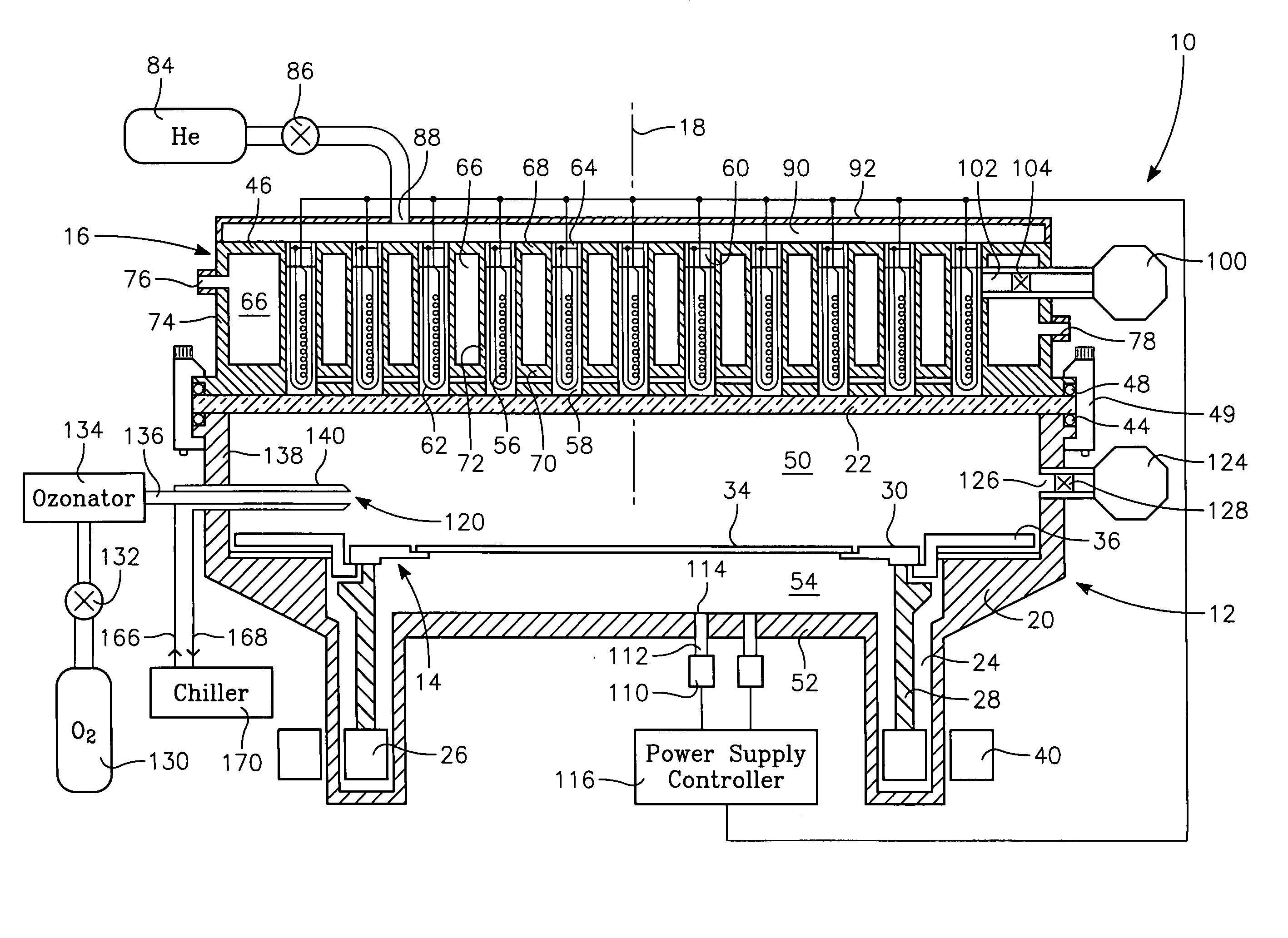
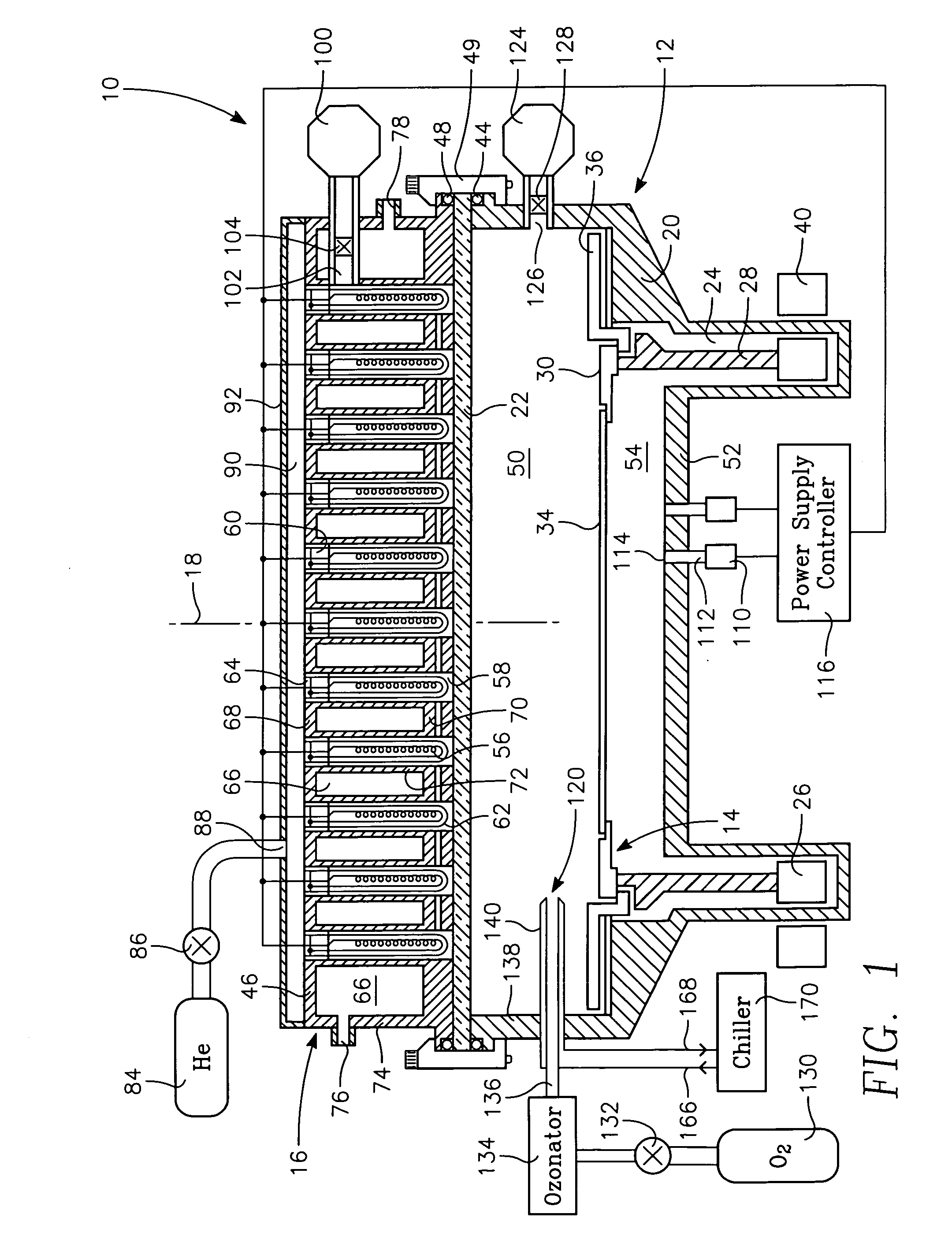
[0026] The invention in part concerns the thermal oxidation of silicon or other materials in the presence of ozone in an RTP (rapid thermal processing) chamber.

[0027]FIG. 1 schematically illustrates in cross section an RTP chamber 10 described by Ranish et al. in U.S. Pat. No. 6,376,804, incorporated herein by reference and generally representative of the Radiance RTP chamber available from Applied Materials, Inc. of Santa Clara, Calif. The RTP chamber 10 includes a vacuum chamber 12, a wafer support 14 located within the chamber 12, and a lamphead 16 or heat source assembly located on the top of the chamber 12, all generally symmetrically arranged about a central axis 18.

[0028] The vacuum chamber 12 includes a chamber body 20 and a window 22 resting on the chamber body 20. The window 22 is composed of a material that is transparent to infrared light, for example, clear fused silica quartz.

[0029] The chamber body 20 may be made of stainless steel and be lined with a quartz liner ...


PUM

PropertyMeasurementUnit
temperatureaaaaaaaaaa

Abstract

A method and apparatus for oxidizing materials used in semiconductor integrated circuits, for example, for oxidizing silicon to form a dielectric gate. An ozonator is capable of producing a stream of least 70% ozone. The ozone passes into an RTP chamber through a water-cooled injector projecting into the chamber. Other gases such as hydrogen to increase oxidation rate, diluent gas such as nitrogen or O2, enter the chamber through another inlet. The chamber is maintained at a low pressure below 20 Torr and the substrate is advantageously maintained at a temperature less than 800° C. Alternatively, the oxidation may be performed in an LPCVD chamber including a pedestal heater and a showerhead gas injector in opposition to the pedestal.

Description

FIELD OF THE INVENTION [0001] The invention relates generally to fabrication of integrated circuits. In particular, the invention relates to thermal oxidation of and other oxygen-based treatment of electronic materials such as silicon. BACKGROUND ART [0002] The fabrication of silicon integrated circuits typically includes one or more steps of forming layers of silicon dioxide, having a general composition of SiO2, although some variation in its stoichiometry is possible. In some applications, dopants are added. For brevity, this material may hereafter be referred to as oxide. Silicon dioxide is a rugged material that bonds well with silicon and is electrically insulating, that is, dielectric. Thicker layers of oxide are typically deposited by spin-on glasses or by chemical vapor deposition, particularly when they form inter-level dielectric layers, which may be formed over metal and other oxide features. However, thin oxide layers formed over silicon may be formed by oxidizing the s...

Claims


Application Information

Patent Timeline
Patent Type & Authority Applications(United States)
IPC IPC(8): H01L21/302C23C16/00
CPCH01L21/0214H01L21/02238H01L21/02249H01L21/67115H01L21/31658H01L21/31662H01L21/67109H01L21/02255
Inventor YOKOTA, YOSHITAKARAMAMURTHY, SUNDARACHUTHARAMAN, VEDAPURAMCZARNIK, CORYBEHDJAT, MEHRANOLSEN, CHRISTOPHER
Owner APPLIED MATERIALS INC
Why Eureka
Try Eureka