Functional organic thin film, organic thin-film transistor, pi-electron conjugated molecule-containing silicon compound, and methods of forming them

a technology of organic thin films and organic thin films, which is applied in the field of functional organic thin films, organic thin films, and electron conjugated molecule-containing silicon compounds, can solve the problems of troublesome manufacturing steps, low strength, and difficult to impart electric conductivity to self-organizing films, etc., to achieve easy crystallization, prevent physical peeling, and simple process
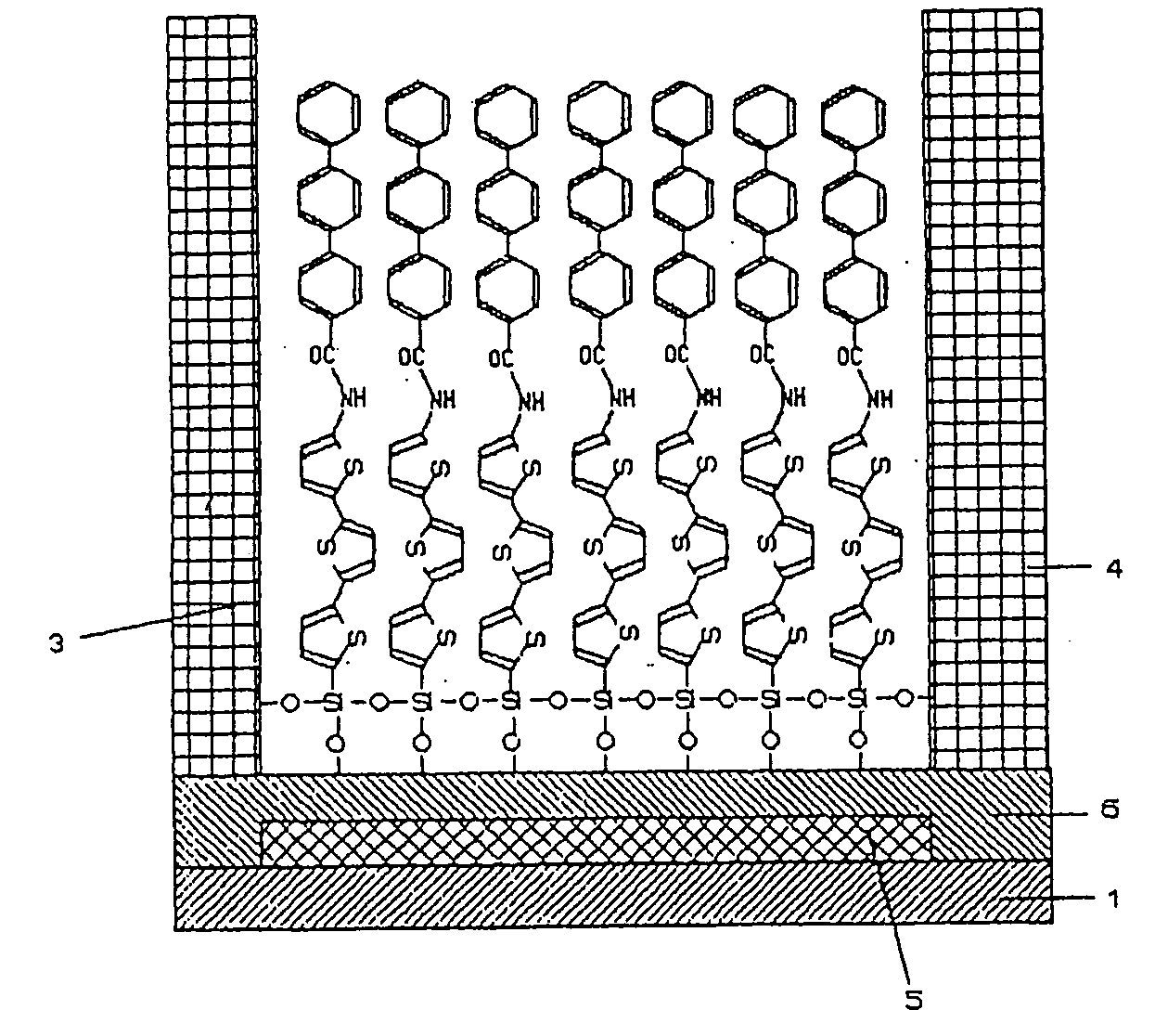
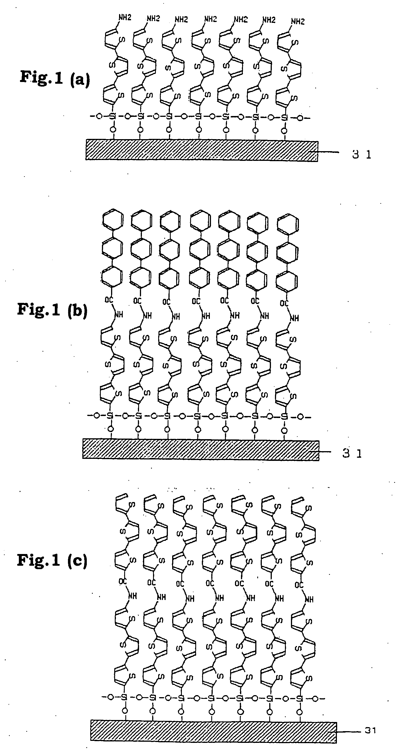
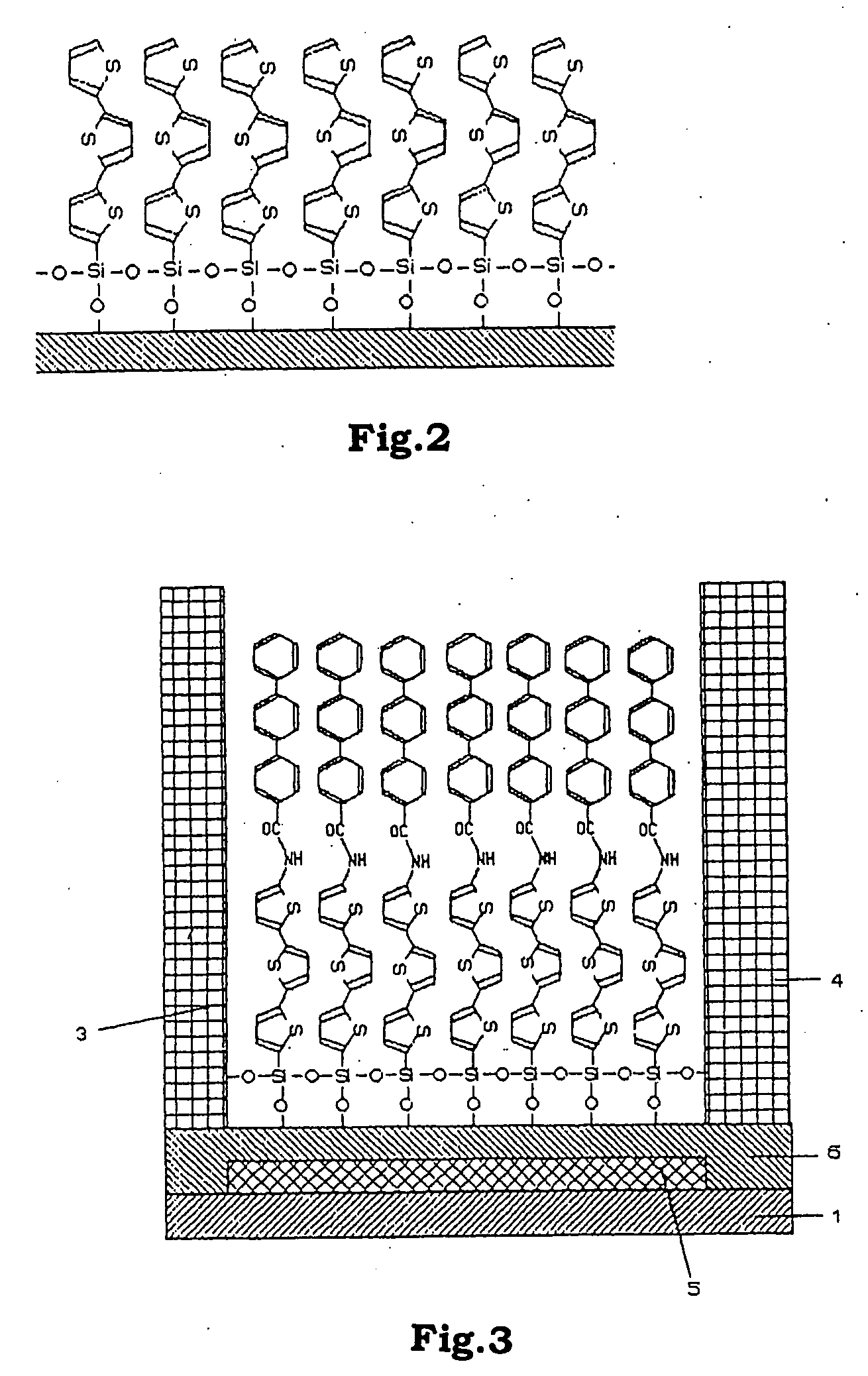
Inactive Publication Date: 2006-10-19
SHARP KK
View PDF7 Cites 19 Cited by
  • Summary
  • Abstract
  • Description
  • Claims
  • Application Information

AI Technical Summary

Benefits of technology

[0013] The present invention was done in view of the aforementioned problems, and an object of the present invention is to provide a compound which can be easily crystallized to form a film by a simple process, in which the resulting film is firmly adsorbed onto a substrate surface to prevent physical peeling, and shows a high ordering property, crystallizability and electric conductive property.
[0015] A further object of the present invention is to provide TFT having high performance and high reliance by maintaining a sufficient carrier mobility and suppressing an off current in TFT using an organic thin film.

Problems solved by technology

However, when the organic compound semiconductor layer for obtaining a higher field-effect mobility than that of the aforementioned amorphous silicon is prepared, it needs a vacuum process such as a resistance heating deposition method and a molecule beam deposition method leading that its manufacturing step becomes troublesome and, at the same time, a film having crystallizability is obtained only under a particular condition.
In addition, the organic compound film is adsorbed onto a substrate by physical adsorption which is low at strength, and is easily peeled.
However, in making the film by physical adsorption, there is no report that compatibility and orientation property of a molecule at an interface between a physical adsorbed organic compound and the substrate can be controlled.
However, although electric conductivity of the self-organizing film is determined by an organic functional group in the silicon-based compound contained in the film, there are no commercially available silane coupling agents which have an organic functional group containing π-electron conjugated molecule and, for this reason, it is difficult to impart electric conductivity to the self-organizing film.
However, although the afore-proposed compounds can manufacture a self-organized film which can be chemically adsorbed onto a substrate, a film having high ordering property, crystallizability and electric conductive property which can be used in an electronic device such as TFT could not be necessarily manufactured.
Further, when the above-proposed compounds are used in a semiconductor layer of organic TFT, there is a problem that an off current becomes great.
However, since only one thiophene molecule which is a functional group contributes to a π-electron conjugation system, there is a problem that intermolecular interaction is weak, and expansion of a π-electron conjugation system indispensable for electric conductivity is very small.
Even when the number of thiophene molecules which are the aforementioned functional group can be increased, it is difficult that a factor forming ordering property of the film can match intermolecular interaction between a long chain alkyl part and a thiophene part.
Further, as electric conductive property, one thiophene molecule which is a functional group, is great at its HOMO-LUMO energy gap and hence there was a problem that even when the molecule is used as an organic semiconductor layer in TFT, sufficient carrier mobility cannot be obtained.

Method used


Image

  • Functional organic thin film, organic thin-film transistor, pi-electron conjugated molecule-containing silicon compound, and methods of forming them
  • Functional organic thin film, organic thin-film transistor, pi-electron conjugated molecule-containing silicon compound, and methods of forming them
  • Functional organic thin film, organic thin-film transistor, pi-electron conjugated molecule-containing silicon compound, and methods of forming them

Examples


example 1

Synthesis of terphenyltrichlorosilane by Grignard Method

[0121] In a 500 ml glass flask equipped with a stirrer, a reflux condenser, a thermometer and a dropping funnel, 1.5 mole of terphenyl was dissolved in carbon tetrachloride, to which NBS and AIBN were added. The mixture was stirred for 3 hours, and filtered under reduced pressure to obtain bromoterphenyl. Subsequently, in a 500 ml glass flask equipped with a stirrer, a reflux condenser, a thermometer and a dropping funnel, 0.5 mole of metal magnesium and 300 ml of THF (tetrahydrofuran) were put, to which 0.5 mole of the bromoterphenyl was dropwise added at 50 to 60° C. over 2 hours using dropping funnel. After the dropping having been completed, the mixture was aged at 65° C. for 2 hours to prepare Grignard reagent.

[0122] In a 1 liter glass flask equipped with a stirrer, a reflux condenser, a thermometer and a dropping funnel, 1.0 mole of SiCl4 (tetrachlorosilane) and 300 ml of toluene were put and cooled with ice, to which t...

example 2

Synthesis of terthiophenetrichlorosilane by Grignard Method

[0130] In a 500 ml glass flask equipped with a stirrer, a reflux condenser, a thermometer and a dropping funnel, 1.0 mole of terthiophene was dissolved in carbon tetrachloride, to which NBS and AIBN were added. The mixture was stirred for 2.5 hours, and filtered under reduced pressure to obtain bromoterthiophene. Subsequently, in a 500 ml glass flask equipped with a stirrer, a reflux condenser, a thermometer and a dropping funnel, 0.5 mole of metal magnesium and 300 ml of THF (tetrahydrofuran) were charged, to which 0.5 mole of bromoterthiophene was dropwise added at 50 to 60° C. over 2 hours using a dropping funnel. After the dropping having been completed, the mixture was aged at 65° C. for 2 hours to prepare Grignard reagent.

[0131] In a 1 liter glass flask equipped with a stirrer, a reflux condenser, a thermometer and a dropping funnel, 1.5 mole of SiCl4 (tetrachlorosilane) and 300 ml of toluene were charged and cooled ...

example 3

Synthesis of terthiophenetrichlorosilane Utilizing Li

[0139] In one liter glass flask equipped with a stirrer, a thermometer and a dropping funnel, 300 ml of a tetrahydrofuran solution containing 1.0 mole of terthiophene was charged and cooled to −78° C., to which 1.0 mole of n-butyllithium was slowly and dropwise added. Then the mixture was stirred for an hour to yield a lithium salt of terthiophene having the structure represented by the formula (a).

[0140] Then, a solution of tetrachlorosilane in tetrahydrofuran was added to the above mixture and was stirred overnight. Lithium chloride, toluene and unreacted tetrachlorosilane were removed from the reaction solution. Thereafter, this solution was distilled to obtain the title compound at a yield of 45%.

[0141] Regarding the resulting compound, its infrared absorption spectrum and nuclear magnetic resonance were measured, and show the absorptions at the same positions as that of the compound shown in Example 2. Thus, it was confir...


PUM

PropertyMeasurementUnit
thicknessaaaaaaaaaa
carbon numberaaaaaaaaaa

Abstract

An organic thin film having both a chemical structure of an organic material that is a factor determining a characteristic of the thin film and a high-order structure of the thin film, for example, the crystallinity of molecules, namely, the orientation. A functional organic thin film composed of molecules the main skeleton structure portion of which is arbitrarily given electrical, optical, electrochemical function and a method for simply forming such a functional organic thin film are also disclosed. The functional organic film is formed of a silicon compound expressed by formula R1—SiX1X2X3 (I) where R is an organic residue which may have a terminal replaced by a functional grou p and to which π-electron conjugate units are bonded, and X1, X2 and X3 are the same group or different groups and given a hydroxyl group by hydrolysis.

Description

TECHNICAL FIELD [0001] The present invention relates to a functional organic thin film, an organic thin film transistor, a π-electron conjugated molecule-containing silicon compound, and a method of forming them. More particularly, the present invention relates to the functional organic thin film using the π-electron conjugated molecule-containing silicon compound having property such as electric conductivity, the organic thin film transistor using the π-electron conjugated molecule-containing silicon compound in a semiconductor layer, the π-electron conjugated molecule-containing silicon compound and the method of forming them. BACKGROUND ART [0002] Recently, semiconductors using organic compounds (organic semiconductor) have been researched and developed, and outcome thereof has been reported. Because when compared with semiconductors of inorganic materials, the organic semiconductors are simple to manufacture, are easy to process, can response to enlargement of a device, can expe...

Claims


Application Information

Patent Timeline
Patent Type & Authority Applications(United States)
IPC IPC(8): H01L51/00H01L51/40C07F7/18C08G77/04C08G77/06C08G77/28C08G77/42C09D183/04H01L29/786H01L51/30
CPCC07B2200/11C07F7/1836C08G77/04C08G77/06H01L51/0545H01L51/0036H01L51/0068H01L51/0094C09D183/04C07F7/1804H10K85/113H10K85/655H10K85/40H10K10/466
Inventor HANATO, HIROYUKINAKAGAWA, MASATOSHITAMURA, TOSHIHIRO
Owner SHARP KK
Why Eureka
Try Eureka