

Ceramic glaze coating structure of a chip element and method of forming the same
- Summary
- Abstract
- Description
- Claims
- Application Information
AI Technical Summary
Benefits of technology
Problems solved by technology
Method used
Image

Examples
first embodiment
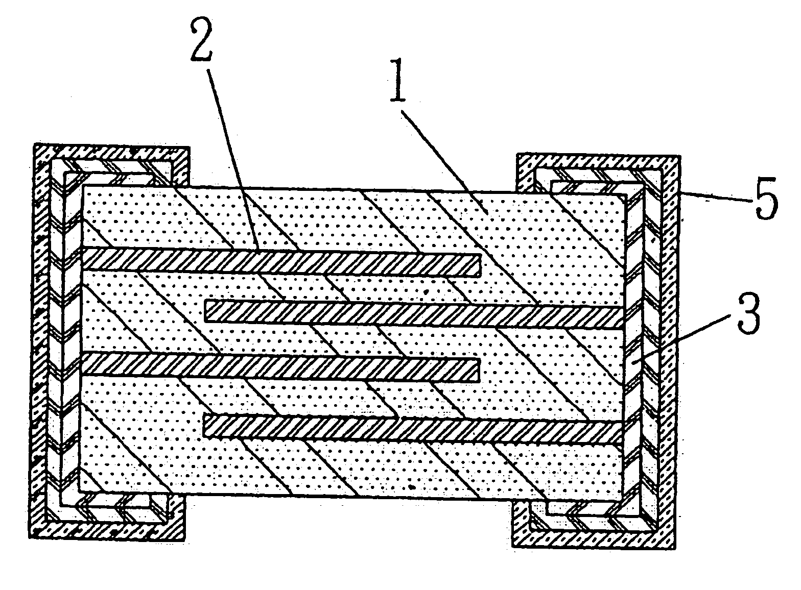
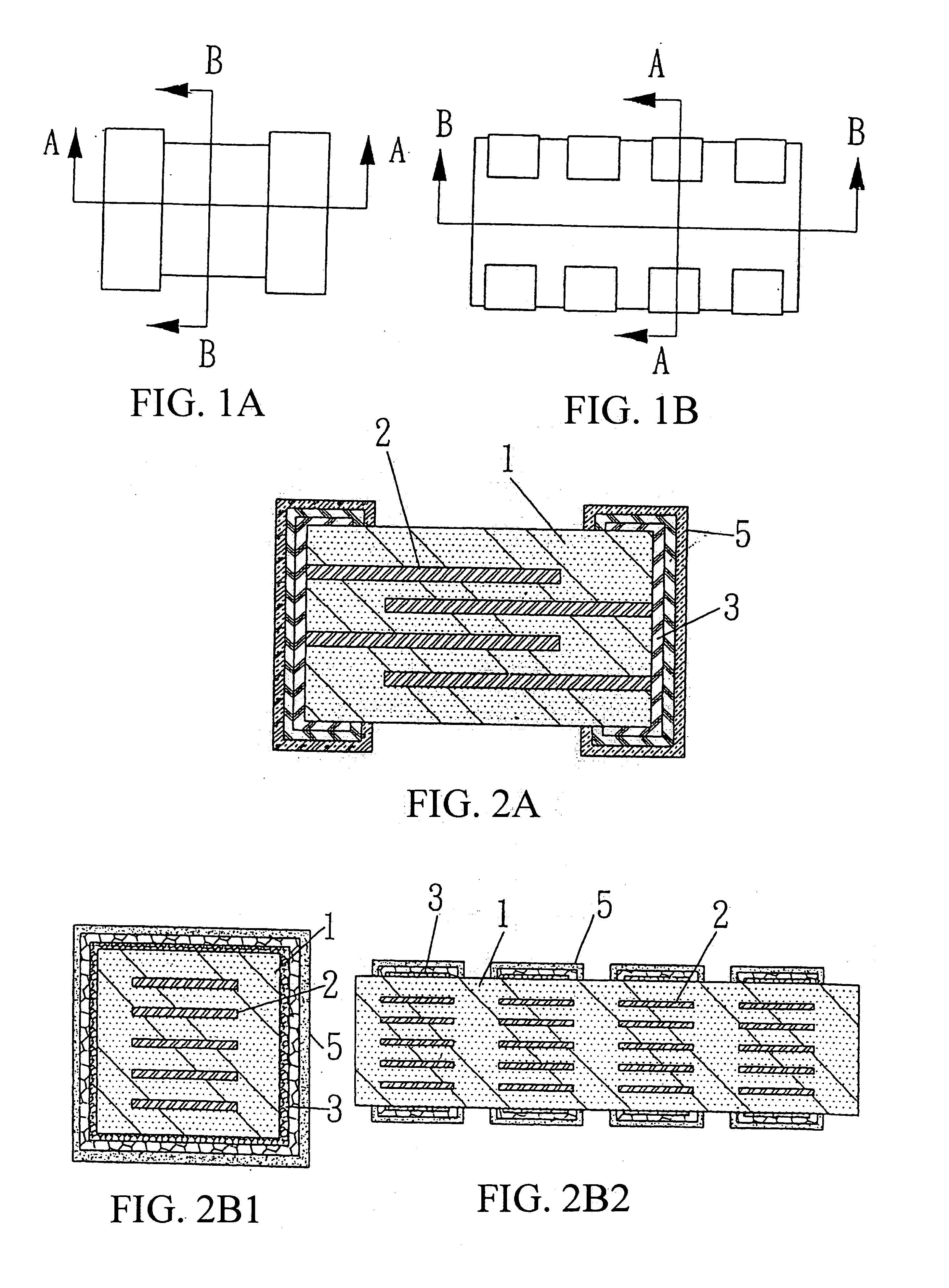
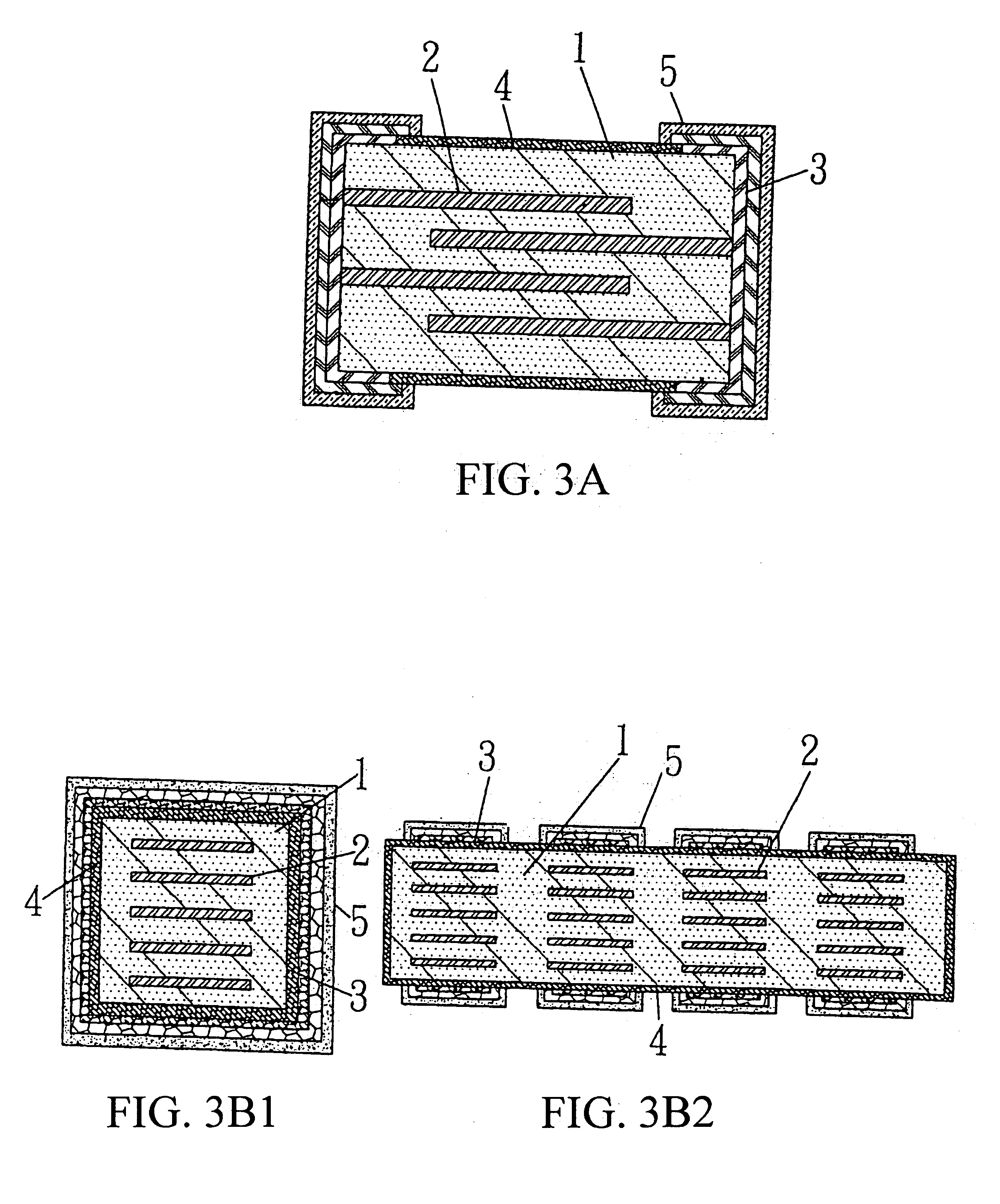
[0049] The method according to the present invention is as shown in FIG. 8A. A step of coating the body with a ceramic glaze is added after completing the step of forming the structure of the electronic element body with the material body 1 and the plurality of inner electrodes 2, and before the step of forming the structure of the plurality of terminal electrodes 3. This coating step is used to apply the ceramic glaze to all the surfaces of the entire element, no matter whether the structure of terminal electrodes 3 is completely or partially formed on the surface. Then, after the high-temperature sintering of the terminal electrodes 3, a plating process that is the same as the process for normal electronic elements is applied to form the terminal electrodes 3 having a plurality of welding interface layers 5 with a desirable welding property.
second embodiment
[0050] The method according to the present invention is as shown in FIG. 8B. A step of coating the body with a ceramic glaze is added after completing the step of forming the structure of the electronic element body having the material body 1 and the plurality of inner electrodes 2, and after completing the step of forming the structure of the plurality of terminal electrodes 3. This coating step is used to apply the ceramic glaze to all the surfaces of the entire element, no matter whether the structure of terminal electrodes 3 is completely or partially formed on the surface. Then, after the high-temperature sintering of the terminal electrodes 3, a plating process that is the same as the process for normal electronic elements is applied to form the terminal electrodes 3 having a plurality of welding interface layers 5 with a desirable welding property.
third embodiment
[0051] The method according to the present invention is as shown in FIG. 8C. After completing the step of forming the structure of the electronic element body with the material body 1 and the plurality of inner electrodes 2, a step of forming the structure of a plurality of terminal electrodes is performed before and after coating the body with the ceramic glaze. This coating step is used to apply the ceramic glaze to all the surfaces of the entire element, no matter whether the structure of the terminal electrodes 3 is completely or partially formed on the surface. Then, after the high-temperature sintering of the terminal electrodes 3, a plating process that is the same as the process for normal electronic elements is applied to form the terminal electrodes 3 having a plurality of welding interface layers 5 with a desirable welding property.
[0052] The present invention has at least the following efficacies.
[0053] 1. The process for forming the ceramic glaze-coating structure of c...
PUM
| Property | Measurement | Unit |
|---|---|---|
| Temperature | aaaaa | aaaaa |
| Temperature | aaaaa | aaaaa |
| Structure | aaaaa | aaaaa |
Abstract
Description
Claims
Application Information