Methods of fabricating nano-scale and micro-scale mold for nano-imprint, and mold usage on nano-imprinting equipment

a nano-imprint and nano-micro-scale technology, applied in nanoinformatics, photomechanical equipment, instruments, etc., can solve the problems of mold release, mold release characteristics not improved, plane pressure irregularities not eliminated, etc., and achieve excellent nano-imprinting

Inactive Publication Date: 2006-11-16
HITACHI IND EQUIP SYST CO LTD
View PDF7 Cites 26 Cited by
  • Summary
  • Abstract
  • Description
  • Claims
  • Application Information

AI Technical Summary

Benefits of technology

[0023] According to the invention, excellent nano-imprinting can be carried out without increasing the release force between the mold and the resin film, which is the transferred material, during nano-imprinting. Moreover, because the nano-imprint face is difficult to subject to damages, a long-life mold for nano-imprint is obtained.

Problems solved by technology

However, when the present inventors investigated the above imprint techniques, which are assumed to be able to form fine patterns, it is found that in the case where Ni is used as the mold, there are problems in releasing the mold from a transferred object after the transfer, as follows.
However, when the present inventors conducted an experiment of transfer by using, as the buffer material, a material softer than the mold and the pressure face, even if the above material is resiliently deformed to fill the gap in between the mold and the pressure face during the pressuring, repulsion from the buffer material becomes consequently large in the portion with a narrow gap as compared with the portions with a wide gap, As a result, it was revealed that in-plane pressure irregularity was not eliminated and the mold-release characteristics was not improved, either.

Method used


Image

  • Methods of fabricating nano-scale and micro-scale mold for nano-imprint, and mold usage on nano-imprinting equipment
  • Methods of fabricating nano-scale and micro-scale mold for nano-imprint, and mold usage on nano-imprinting equipment
  • Methods of fabricating nano-scale and micro-scale mold for nano-imprint, and mold usage on nano-imprinting equipment

Examples


example 1

[0093] The characteristic of the surface oxide-film of a Ni mold, which is one of the embodiments of the invention, will be described using FIG. 4 and FIG. 5. In the Ni mold, just before applying a release agent, an oxide film formed by natural oxidation or an oxide film formed by an oxidation treatment, the oxide film being present in the surface, is treated with acid cleaning. In the case where a hydrochloric acid is used as the acid-cleaning chemical, a solution of 0.5-10% by weight concentration is preferable, and a solution of 1-5% by weight concentration is preferable in particular. In the case where a sulfuric acid is used as the acid-cleaning chemical, a solution of 0.5-3% by weight concentration is preferable, and a solution of 0.5-2% by weight concentration is preferable in particular. Preferably, the temperature for the acid cleaning is 20-27° C., and the acid-cleaning time is 20-50 sec. Because these conditions vary depending on the quality of materials of the mold to be...

example 2

[0101] The force required for the release between the mold and the transferred substrate, which is one of the embodiments of the invention, will be described using FIGS. 7 and 8. The mold was produced using the same method as that of the embodiment 1, and the force required for the mold-release of the mold and the substrate was measured with a tensile test machine. FIG. 7 shows the force required during the mold release against the Ni-oxide film thickness in the mold surface. It was found that as the thickness of a Ni-oxide film becomes thinner, it can be released with a lower force. FIG. 8 shows the force required during the mold release against the sum of the thickness of the Ni-oxide film in the mold surface, and the thickness of the release agent. The data of FIG. 7 and FIG. 8 were obtained through observations by TEM, and the measurements by the tensile test machine. It turned out that as the sum of the thickness of the Ni-oxide film and the thickness of a mold-release agent be...

example 3

Biotechnology (Immunity) Chip

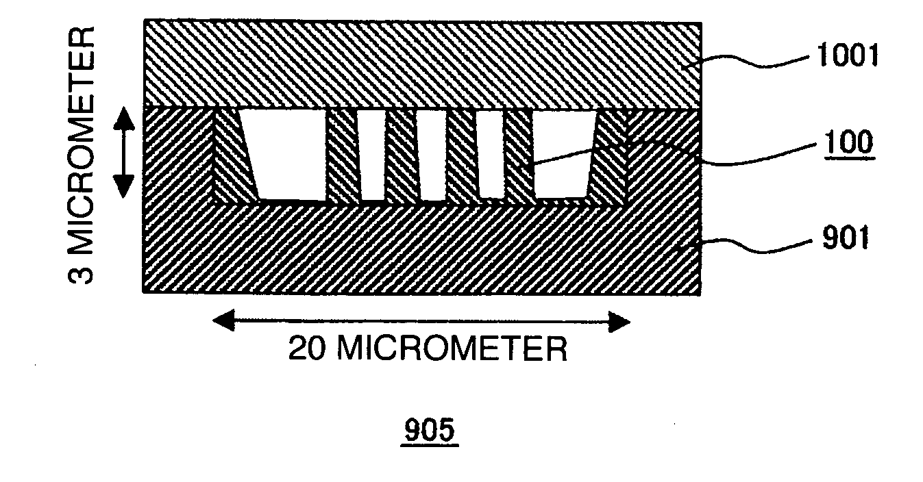
[0103] The invention is applied to a mold used for biochip preparation. FIG. 9 is a schematic view of a biochip 900. The biochip 900 has a structure wherein a passage 902 with a depth of 3 um and a width of 20 um is formed in a glass substrate 901, and a sample containing DNA (deoxyribonucleic acid), blood, protein, or the like is introduced from a lead-in hole 903, and flown through the passage 902, and then flown to a discharge orifice 904. A molecule filter 905 is installed in the passage 902. A protrusion assembly 100 with a diameter of 250 nm to 300 nm and a height of 3 um is formed in the molecule filter 905.

[0104]FIG. 10 is a cross-sectional bird's-eye view around a portion in which the molecule filter 905 is formed. The passage 902 is formed in the substrate 901, and the protrusion assembly 100 is formed in part of the passage 902. The substrate 901 is covered with an upper substrate 1001, and the sample will move inside the passage 902. For ex...


PUM

PropertyMeasurementUnit
thicknessaaaaaaaaaa
contact angleaaaaaaaaaa
thicknessaaaaaaaaaa

Abstract

To provide a metal mold excellent in the mold-release characteristic and the transfer accuracy in a nano-imprint method. By controlling the thickness of a metal oxide film formed in the face of a release agent and a mold, the adhesive amount of the release agent layer formed in the outer layer thereof is adjusted, thereby forming a mold excellent in the mold-release characteristic. The present invention also relates to methods of fabricating molds for nano-imprint, and mold usage on nano-imprinting equipment.

Description

FIELD OF THE INVENTION [0001] The present invention relates to a mold for nano-imprint wherein a fine structure is formed on a transferred substrate, which is made of resin, using a mold for forming nano meter level fine convexo-concaves, and to methods of fabricating the same, nano-imprinting equipment, and methods of nano-imprinting. BACKGROUND OF THE INVENTION [0002] Recently, miniaturization and more integration of semiconductor integrated circuits have been progressing, and as a pattern transfer technique for realizing the fine process, higher precision of the photolithography equipment has been progressing. However, the processing method thereof has come near the wavelength of light sources in the light exposure, and the lithography technique has come near the limitations. Therefore, in order to advance the miniaturization and higher precision further, the electron beam lithography equipment, which is a type of charged particle beam equipment, is beginning to be employed inste...

Claims


Application Information

Patent Timeline
Patent Type & Authority Applications(United States)
IPC IPC(8): H01L21/302B81C99/00B29C33/38B29C59/02G11B5/84H01L21/027
CPCB81C1/0046B81C99/009G11B5/855B82Y40/00G03F7/0002B82Y10/00
Inventor OHASHI, KENYAMIYAUCHI, AKIHIROOGINO, MASAHIKO
Owner HITACHI IND EQUIP SYST CO LTD
Why Eureka
Try Eureka