Method for fabricating a multilayer wiring board, multilayer wiring board, and electronic device using the same

Inactive Publication Date: 2007-02-15
HITACHI CABLE +1
View PDF3 Cites 19 Cited by
  • Summary
  • Abstract
  • Description
  • Claims
  • Application Information

AI Technical Summary

Benefits of technology

[0125] (1) In the first preferred embodiment, the photosensitive plating resist is etched for forming the wiring pattern, not like the conventional subtractive process in which the wiring layer is removed by the chemical etching. Accordingly, the formation limit of the wiring pitch can be determined based on the resolution of the photosensitive plating resist, so that the wiring density can be improved to be narrower than 40 μm pitch. Therefore, in comparison with the conventional subtractive process, the wiring density can be improved.
[0126] Furthermore, the side etching occurs in the conventional subtractive process, an edge of the surface wiring layer has a trapezoidal cross section, so that the wiring width and the wiring interval in the finished state are fluctuated from the design values of the wiring width and the wiring interval. However, according to the wiring formation in this preferred embodiment, the edge of the surface wiring layer has a rectangular cross section, and the wiring width and the wiring interval are equal to the mask

Problems solved by technology

However, the improvement of the wiring width and the wiring interval between the wiring conductors of the TAB tape using the subtractive process almost reaches to the technical limit.
In addition, in the subtractive process, there is a basic problem in that the wiring width is reduced in accordance with the progress of the etching (side-etching phenomenon).
The photoresist is exfoliated due to the reduction in the wiring width, and chemical dissolution of the copper foil begins from the exfoliated part, as a result, defectiveness of the wiring due to the breaking of wire occurs.
In addition, the wiring interval is increased by the reduction in the wiring adversely, so that a required wiring width is hardly obtained.
However, the wiring width and the wiring interval of an etched product should be measured many times to be fed back to the photomask preparation, thereby causing the complication of the manufacturing process and the obstacle for shortening the product delivery date.
The plating solution to be used is expensive, in addition, the crystallization speed is 1/10 or less of the ordinary electroplating.
Name

Method used


Image

  • Method for fabricating a multilayer wiring board, multilayer wiring board, and electronic device using the same
  • Method for fabricating a multilayer wiring board, multilayer wiring board, and electronic device using the same
  • Method for fabricating a multilayer wiring board, multilayer wiring board, and electronic device using the same

Examples


first preferred embodiment

[0108] (Structure of a Double-Sided Wiring Board)

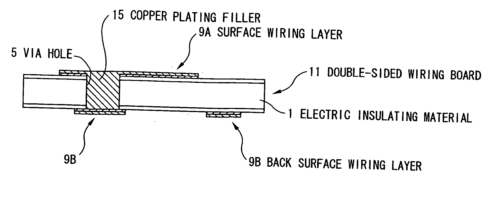
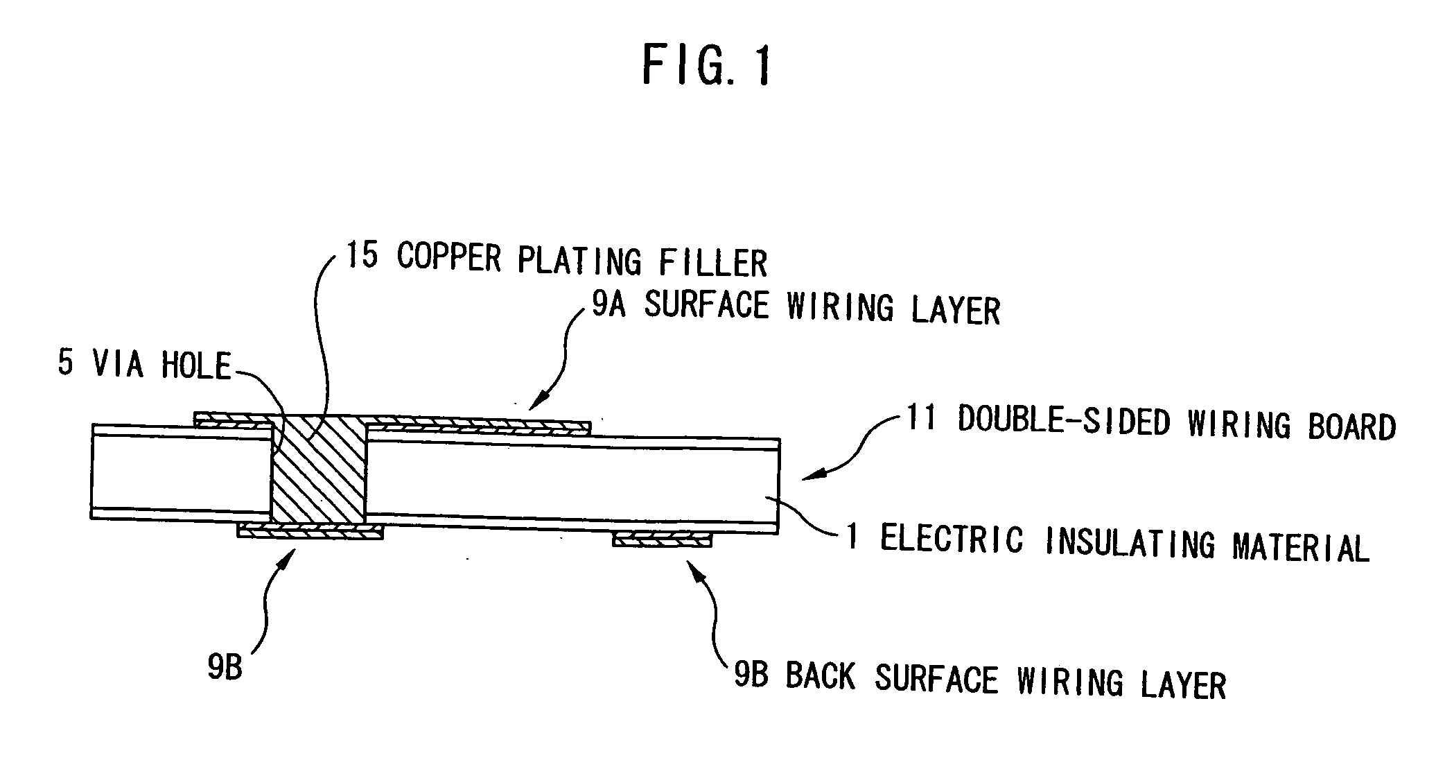
[0109]FIG. 1 shows a cross sectional view of a double-sided wiring board in the first preferred embodiment according to the present invention.

[0110] A double-sided wiring board 11 comprises an electric insulating material 1, a via hole 5 penetrating through the electric insulating material 1 from a front surface to a back surface, a copper plating filler 15 for filling the via hole 5, a surface wiring layer 9A formed on the front surface, and a back surface wiring layer 9B formed on the back surface.

[0111] (Method for Fabricating the Double-Sided Wiring Board)

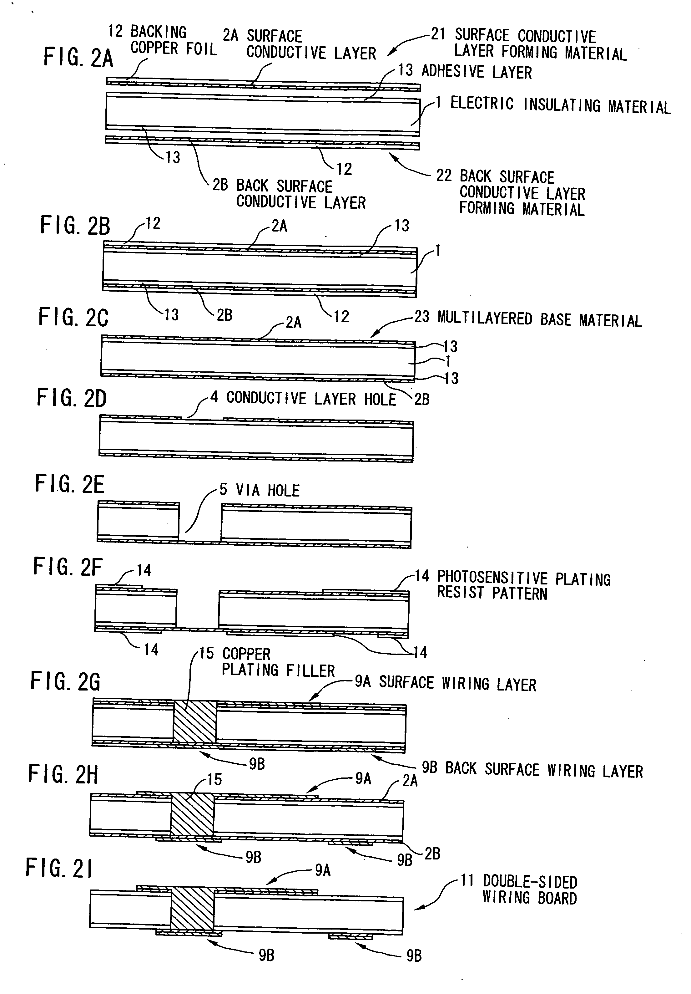
[0112] Based on FIGS. 2A to 2I, a method for fabricating the double-sided wiring board shown in FIG. 1 is explained.

[0113] At first, for an electric insulating material 1 shown in FIG. 2A, a high heat-resistant material composed of, for example, polyimide is prepared. For the case using a TAB tape, it is possible to use a polyimide tape generally having a width of 35, 70, or...

example 1

[0130] A double-sided wiring board 11 was fabricated by the method for fabricating a double-sided wiring board in the first preferred embodiment shown in FIGS. 2A to 2I.

[0131] On one surface of a backing copper foil 12 with a thickness of 18 μm and a width of 26.5 mm, a chromium electroplating layer is formed to have a thickness of 0.02 μm. Then a surface conductive layer 2A is formed to have a thickness of 2 μm by the electrolytic copper plating using a copper sulfate plating bath to provide a surface conductive layer forming material 21. In similar manner, a back surface conductive layer 2B is formed to have a thickness of 2 μm to provide a back surface conductive layer forming material 22 (FIG. 2A).

[0132] Next, both surfaces of an electric insulating material 1 composed of a polyimide tape with a thickness of 25 μm and a width of 35 mm are sandwiched by the surface conductive layer forming material 21 and the back surface conductive layer forming material 22 via an epoxy system...

third preferred embodiment

[0153] (Structure of a Double-Sided Wiring Board)

[0154]FIG. 5 shows a cross sectional view of a double-sided wiring board in the third preferred embodiment according to the present invention.

[0155] A double-sided wiring board 41 comprises a photosensitive permanent resist 16, a photosensitive permanent resist hole 17 penetrating through the photosensitive permanent resist 16 from a front surface to a back surface, a copper plating filler 15 for filling the photosensitive permanent resist hole 17, a surface wiring layer 9A formed on the front surface of the photosensitive permanent resist 16, and a back surface wiring layer 10 formed on the back surface of the photosensitive permanent resist 16.

[0156] (Method for Fabricating the Double-Sided Wiring Board)

[0157] Based on FIGS. 6A to 6J, a method for fabricating the double-sided wiring board shown in FIG. 5 is explained.

[0158] At first, as shown in FIG. 6A, the photosensitive permanent resist 16 is applied to the back surface copp...


PUM


Abstract

On both surfaces of an electric insulating material 1, a surface conductive layer 2A and a back surface conductive layer 2B are formed by transcription. Further, a via hole 5 penetrating through the surface conductive layer 2A and the electric insulating material 1 is provided. After forming a photosensitive plating resist pattern 14, the via hole 5 is filled with a copper plating filler 15, and the surface wiring layer 9A and the back surface wiring layer 9B are formed. Thereafter, the photosensitive plating resist pattern 14 as well as the surface conductive layer 2A and the back surface conductive layer 2B provided under the photosensitive plating resist pattern 14 are removed to fabricate a double-sided wiring board 11.

Description

[0001] The present application is based on Japanese Patent Application No. 2005-323156 filed on Nov. 8, 2005, the entire contents of which are incorporated herein by reference. BACKGROUND OF THE INVENTION [0002] 1. Field of the Invention [0003] The invention relates to a method for fabricating a multilayer wiring board on which a semiconductor device, passive element electronic parts, functional elements or the like are mounted, a multilayer wiring board, and an electronic device using the same. [0004] 2. Description of the Related Art [0005] In these days, it is desired that the electronic parts such as a semiconductor device, resistor, capacitor or the like are miniaturized and slimmed, for realizing the light-weighting of electronic apparatus such as a digital still camera, a video camera, and a cellular phone. For example, as to the resistor and capacitor, a 0603 (0.6 mm×0.3 mm) microchip resistors are put to practical use. In addition, as to the semiconductor chip, a bare chip ...

Claims


Application Information

Patent Timeline
IPC IPC(8): C25D5/02
CPCH05K3/0023H05K3/025H05K3/108H05K3/386H05K3/421H05K3/423H05K3/427H01L2924/0002H05K3/4652H05K2201/0355H05K2201/0394H05K2203/0733H01L2924/00
Inventor CHINDA, AKIRAMIYAMOTO, NOBUAKIMITA, MANORU
Owner HITACHI CABLE
Why Eureka
Try Eureka