Optical semiconductor devices on InP substrate

a technology of optical semiconductors and inp substrates, applied in semiconductor devices, semiconductor lasers, lasers, etc., can solve the problems of insufficient material exploitation, insufficient performance to realize the practical application of the material, and insufficient research and development, so as to achieve the effect of high practicability

Inactive Publication Date: 2007-03-08
SOPHIA UNIVERSITY +2
View PDF3 Cites 12 Cited by
  • Summary
  • Abstract
  • Description
  • Claims
  • Application Information

AI Technical Summary

Benefits of technology

[0020] Moreover, it is another object of the present invention to provide a p-type semiconductor layer structure with which an optical semiconductor element and device can be readily manufactured each of which has satisfactory characteristics such as light emitting characteristics, high reliability and a long lifetime.
[0027] More generally, in the semiconductor light emitting element and the photo-detecting device, the defects are propagated and diffused from the area having a maximum number of crystal defects due to an influence of the heat, electric conduction, strain and the like to finally reach the light emitting area (active area), thereby causing degradation of the element and ending the element lifetime. When the semiconductor optical element is manufactured, it is necessary to exclude an adverse influence exerted on the element having the crystal defects or to reduce the adverse influence exerted thereon.
[0030] Such a semiconductor layer can be formed and thus is used in manufacturing of the element, which results in that it is possible to realize the manufacturing of the semiconductor device, the laser diode and the light emitting diode which have been conventionally unable to be realized and which, for example, emits light with a wavelength corresponding to yellow light to green light.
[0031] According to the present invention, it is possible to realize the Optical Semiconductor Devices which has higher practicability than that of the conventional one.

Problems solved by technology

However, with regard to the semiconductor devices for emitting light with a wavelength corresponding to yellow light to green light which is about a 500 nm band and is an intermediate wavelength band between a wavelength band of red light and a wavelength band of blue light, the material exploitation has not been sufficiently performed, not to mention the research and development.
For this reason, in particular, with respect to the laser diode, the performance enough to realize its practical application has not yet been realized.
In general, however, since a p-type conductivity property is difficult to control, a p-type semiconductor layer of a pn junction type semiconductor device can be realized only when limited kinds of group II-VI compound semiconductors such as ZnSe are used.
In the group II-VI compound semiconductors, in general, as a band gap width becomes wider, a p-type carrier concentration decreases, resulting in that any of these group II-VI compound semiconductors cannot be utilized in the pn junction type semiconductor device.
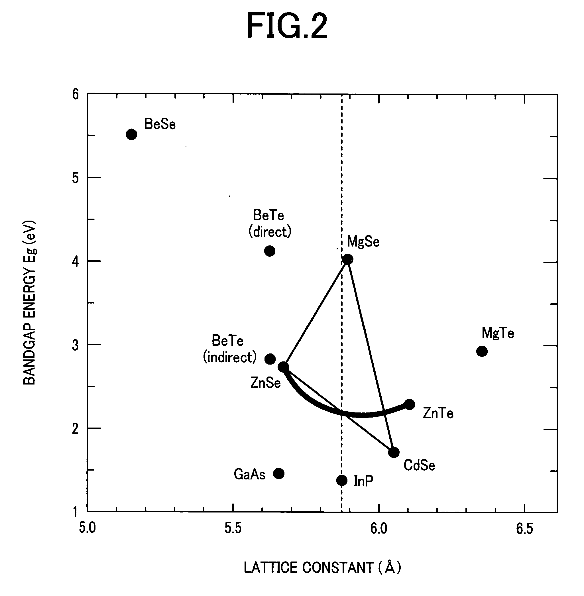
It is considered that the main cause for which the laser oscillation is not obtained is due to difficulty in p-type conductivity controlled by impurity doping into MgxZnyCd1-x-ySe.
However, with regard to a p-type conductivity control, a p-type carrier concentration of 1×1017 cm−3 or more which is required for the laser diode has not yet been reported.
However, it is considered that the cause may be that at least an ideal impurity dopant which is replaced with a part of atoms arranged in the MgxZnyCd1-x-ySe crystal to be stably present in the crystal and which efficiently discharges holes with low energy, has not yet been found out, or is not present.
This is an essential problem in characteristics which MgxZnyCd1-x-ySe has.
However, the sufficient characteristics have not yet been obtained.

Method used


Image

  • Optical semiconductor devices on InP substrate
  • Optical semiconductor devices on InP substrate
  • Optical semiconductor devices on InP substrate

Examples


first embodiment

[0084] the present invention will be described below. A specimen shown in FIG. 5A was manufactured, and its characteristics were evaluated.

[0085] A crystal of the specimen shown in FIG. 5A was grown by using a 2-growth chamber molecular beam epitaxy (MBE) system. First, an InP substrate 21, after being subjected to the optimal surface treatment, was placed within the MBE system. The InP substrate 21 was then placed in a preparatory chamber for specimen exchange, air therein was vacuumed by a vacuum pump, until a pressure of 10−3 Pa or less was obtained, and the InP substrate 21 was heated up to 100° C. to desorb residual moisture and an impurity gas.

[0086] Next, the InP substrate 21 was conveyed to a III-V dedicated growth chamber, and was heated at a substrate temperature of 500° C. while a P molecular beam is applied to the surface of the InP substrate 21, thereby removing an oxide film formed on the surface of the InP substrate 21. After that, an InP buffered layer 22 was grown ...

second embodiment

[0100] the present invention will be described below. Specimens shown in FIGS. 8A and 8B were manufactured, and their characteristics were evaluated.

[0101] The specimen shown in FIG. 8A will now be described. The specimen was manufactured through the crystal growth by using the 2-growth chamber molecular beam epitaxy (MBE) system. An InP substrate 21, after having been subjected to the optimal surface treatment, was placed within the MBE system. The InP substrate 21 was then placed in a preparatory chamber for specimen exchange, air therein was vacuumed by a vacuum pump, until a pressure of 10−3 Pa or less was obtained, and the InP substrate 21 was heated up to 100° C. to desorb residual moisture and an impurity gas.

[0102] Next, the Inp substrate 21 was conveyed to a III-V dedicated growth chamber, and was heated at a substrate temperature of 500° C. while a P molecular beam is applied to the surface of the Inp substrate 21, thereby removing an oxide film formed on the surface of t...

third embodiment

[0114] the present invention will now be described. A specimen shown in FIG. 11 was manufactured and its characteristics were evaluated. A crystal of the specimen shown in FIG. 11A was grown by using a 2-growth chamber molecular beam epitaxy (MBE) system. First, an S-doped InP substrate 21, after being subjected to the optimal surface treatment, was placed within the MBE system. The InP substrate 21 was then placed in a preparatory chamber for specimen exchange, air therein was vacuumed by a vacuum pump, until a pressure of 10−3 Pa or less was obtained, and the InP substrate 21 was heated up to 100° C. to desorb residual moisture and an impurity gas.

[0115] Next, the InP substrate 21 was conveyed to a III-V dedicated growth chamber, and heated at a substrate temperature of 500° C. while a P molecular beam is applied to the surface of the InP substrate 21, thereby removing an oxide film formed on the surface of the InP substrate 21. After that, an InP buffered layer 22 was grown to be...


PUM


Abstract

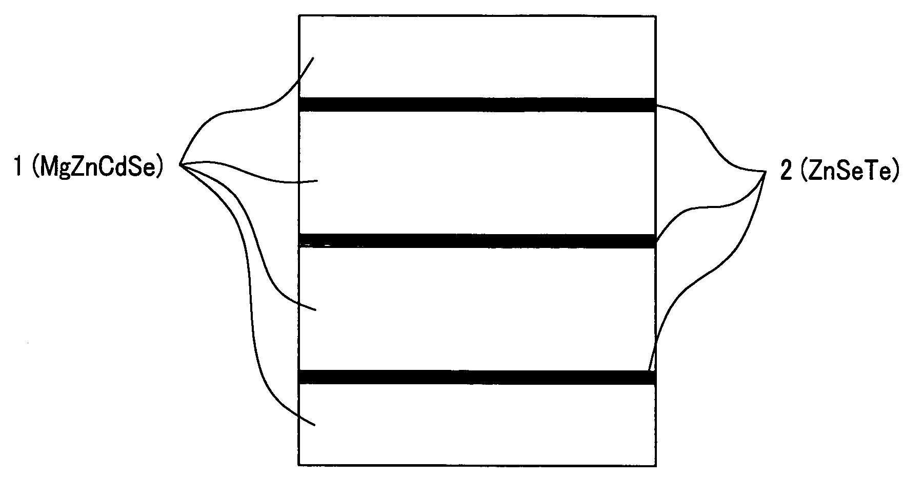
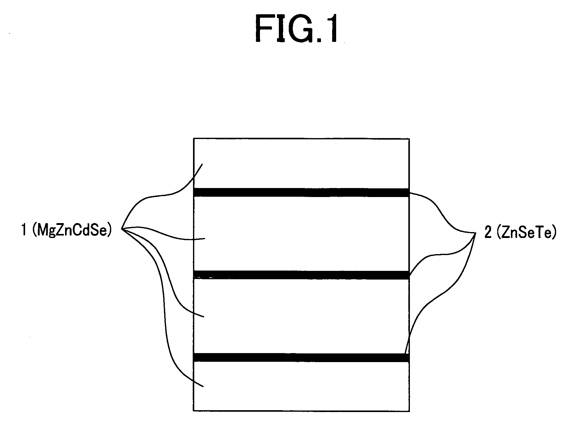
The present invention aims at providing a structure in which a high p-type carrier concentration of 1×1017 cm−3 or more is obtained in a material in which, although it shows normally p-type conductivity, a carrier concentration smaller than 1×1017 cm−3 is only obtained. Also, the present invention aims at providing highly reliable semiconductor element and device each of which has excellent characteristics such as light emitting characteristics and a long lifetime. Each specific layer, i.e., each ZnSe0.53Te0.47 layer (2ML) is inserted between host layers, i.e., Mg0.5Zn0.29Cd0.21Se layers (each having 10ML (atomic layer) thickness) each of which is lattice matched to an InP substrate. In this case, each specific layer in which a sufficient carrier concentration of 1×1018 cm−3 or more is obtained when a single layer is inserted at suitable intervals. As a result, a sufficient hole concentration of 1×1017 cm−3 or more is obtained in the overall crystal in a material in which a hole concentration smaller than 1×1017 cm−3 has been only conventionally obtained.

Description

CLAIM OF PRIORITY [0001] The present application claims priority from Japanese application JP 2005-256566 filed on Sep. 5, 2005, the content of which is hereby incorporated by reference into this application. FIELD OF THE INVENTION [0002] The present invention relates to an optical semiconductor devices on an InP substrate. In particular, the invention relates to an Optical Semiconductor Devices having a p-type cladding layer or the like in which a sufficient p-type carrier concentration (of 1×1017 cm−3 or more) and a wide band gap can be obtained by inserting semiconductor layers, in which a p-type high carrier concentration can be obtained, between semiconductor cladding layers or the like, for which heavy doping is difficult to perform in a compound semiconductor which is mainly constituted by a group II element and a group VI element although it has a wide band gap. [0003] Also, the invention relates to an optical element such as a semiconductor laser diode (LD), a light emittin...

Claims


Application Information

Patent Timeline
Patent Type & Authority Applications(United States)
IPC IPC(8): H01L29/06H01L33/28H01S5/347
CPCB82Y20/00H01L31/0296H01L31/035236H01S2304/02H01L33/28H01S5/0218H01S5/347H01L33/06H01S5/00
Inventor KISHINO, KATSUMINOMURA, ICHIROTAMAMURA, KOSHINAKAMURA, HITOSHI
Owner SOPHIA UNIVERSITY
Why Eureka
Try Eureka