Semiconductor device and method of fabricating the same

Inactive Publication Date: 2007-03-08
PANASONIC CORP
View PDF21 Cites 49 Cited by
  • Summary
  • Abstract
  • Description
  • Claims
  • Application Information

AI Technical Summary

Benefits of technology

[0026] The step (A) may include: preparing a SGOI substrate; and using a buried oxide film of the SGOI substrate as the first insulating layer and a silicon-germanium layer of the SGOI substrate as a layer of the first semiconductor. This feature makes it possible to easily fabricate a semiconductor device having a channel partially formed of strained silicon.
[0027] The step (A) may include: preparing a substrate obtained by epitaxially growing

Problems solved by technology

One of the causes of such acceleration is that it has become more difficult to obtain satisfactory current driving ability than before due to source voltage scaling, deterioration of carrier mobility and the like.
However, under acceleration of miniaturization it becomes very difficult

Method used


Image

  • Semiconductor device and method of fabricating the same
  • Semiconductor device and method of fabricating the same
  • Semiconductor device and method of fabricating the same

Examples


first embodiment

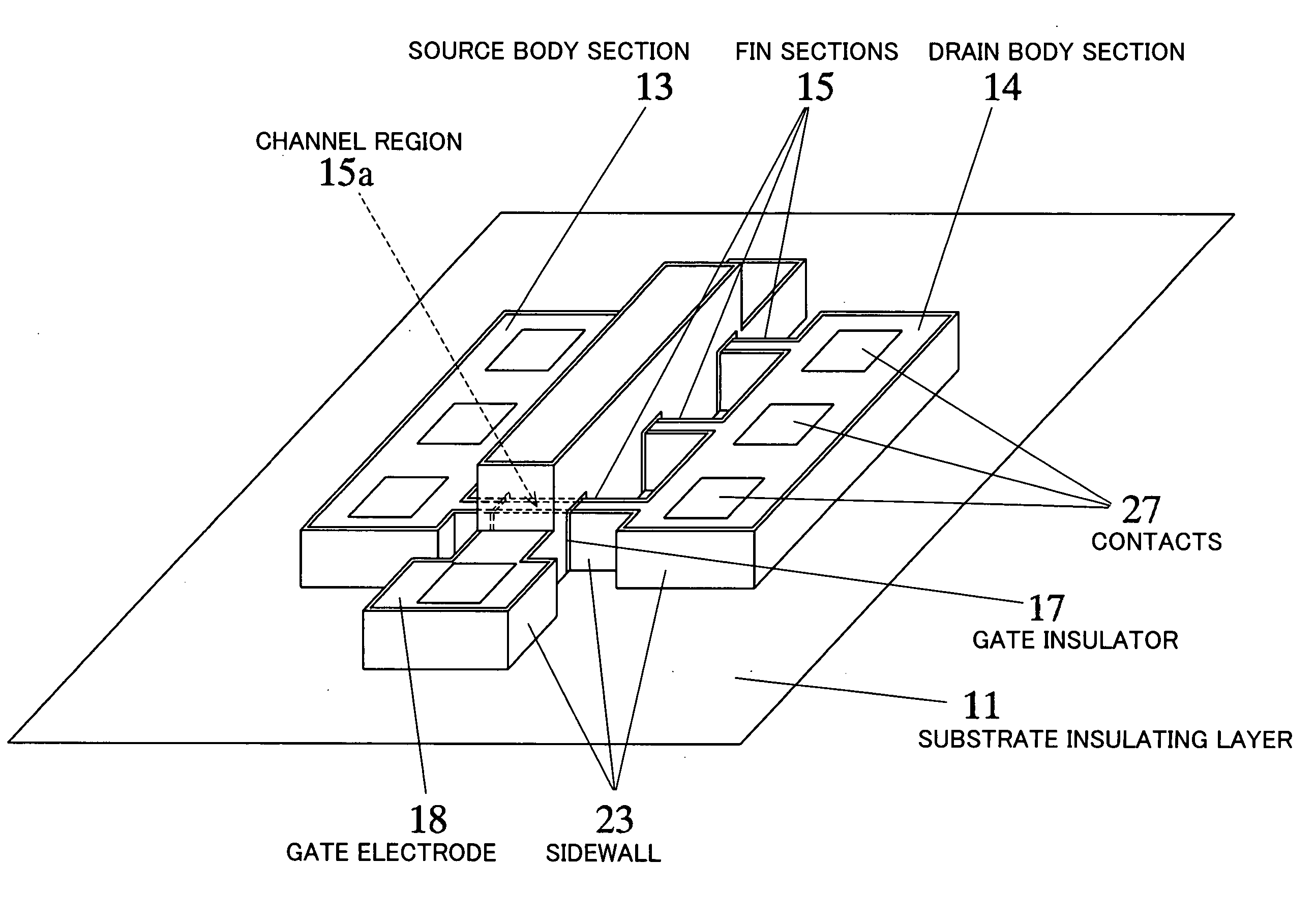
[0050]FIG. 1 is a perspective view schematically showing the construction of a semiconductor device according to a first embodiment of the present invention.

[0051] As shown in FIG. 1, the semiconductor device according to this embodiment comprises a fin FET having as major components thereof a source body section (first body section) 13, a drain body section (second body section) 14, a fin section (connecting section) 15, a gate insulator (second insulating layer) 17, and a gate electrode 18. In FIG. 1, such components as a silicide layer, an interlayer insulator and interconnections are not shown.

[0052] The source body section 13 and the drain body section 14 are each formed into a rectangular parallelepiped shape and are positioned opposite to each other on a substrate insulating layer 11. A plurality of (three in the figure) plate-shaped fin sections 15 stand as spaced from each other on the substrate insulating layer (first insulating layer) in such a manner that the opposite ...

first example

[0084] Hereinafter, a semiconductor device and a fabrication method thereof according to a first example will be described with reference to FIGS. 4A to 8C.

[0085] A semiconductor substrate 101 is prepared in the process illustrated in FIGS. 4A to 4C. Used as the semiconductor substrate 101 is, for example, a SGOI (Silicon Germanium on Insulator) substrate comprising a silicon layer 10, a buried oxide film (substrate insulating layer (thickness: not more than substantially 400 nm)), and a lattice-relaxed silicon-germanium layer 12′ (germanium concentration: 30%, thickness: 100 nm) formed on the buried oxide film.

[0086] In the subsequent process steps illustrated in FIGS. 5A to 5C, firstly, a device region is defined. Specifically, a silicon oxide film, which has been deposited over the entire substrate surface by plasma CVD (Chemical Vapor Deposition) at substantially 600° C., is patterned into a hard mask by dry etching with a resist mask. A size of the hard mask is possible to ad...

second embodiment

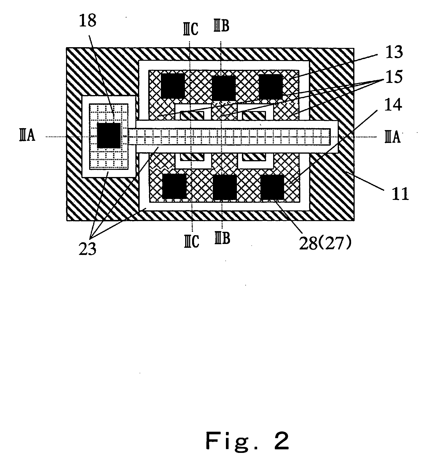
[0100]FIG. 10 is a plan view showing the construction of a semiconductor device according to a second embodiment of the present invention; and FIGS. 11A to 11C are sectional views taken on lines XIA-XIA, XIB-XIIB and XIC-XIC, respectively, of FIG. 10. FIGS. 11A to 11C are drawn by appropriately reducing or enlarging the horizontal dimensions (parallel with the principal surface of a substrate 101) of the semiconductor device shown in the plan view at FIG. 10. Like reference characters designate like or corresponding parts throughout FIGS. 10 and 11A to 11C and FIGS. 2 and 3A to 3C.

[0101] The present embodiment is different from the first embodiment in the following points. The first point is that the relaxed SiGe layer 12 according to the first embodiment is replaced with a strainless silicon layer (hereinafter will be referred to as a relaxed Si layer) 33 and a strained silicon-germanium layer (hereinafter will be referred to as a strained SiGe layer) 30. The second point is that ...


PUM


Abstract

A semiconductor device according to this invention includes: a first insulating layer (11); a first body section (13) including an island-shaped semiconductor formed on the first insulating layer; a second body section (14) including an island-shaped semiconductor formed on the first insulating layer; a ridge-shaped connecting section (15) formed on the first insulating layer to interconnect the first body section and the second body section; a channel region (15a) formed by at least a part of the connecting section in lengthwise direction of the connecting section; a gate electrode (18) formed to cover a periphery of the channel region, with a second insulating layer intervening therebetween; a source region formed to extend over the first body section and a portion of the connecting section between the first body section and the channel region; and a drain region formed to extend over the second body section and a portion of the connecting section between the second body section and the channel region, wherein a semiconductor forming the channel region has a lattice strain.

Description

TECHNICAL FIELD [0001] The present invention relates to a semiconductor device and a method of fabricating the same and, more particularly, to a semiconductor device comprising a fin FET including a semiconductor layer having lattice strain and a method of fabricating such a semiconductor device. BACKGROUND ART [0002] With the trend toward a ubiquitous network and wearable mobile equipment, the market is strongly demanding that LSIs and memory devices exhibit higher speed operation, higher integration and lower power consumption. According to the International Technology Roadmap for Semiconductors (ITRS2001), alternation of design rule generations will be accelerated and, as well, introduction of new materials and structures will start being accelerated at a node below approximately 65 nm node. One of the causes of such acceleration is that it has become more difficult to obtain satisfactory current driving ability than before due to source voltage scaling, deterioration of carrier ...

Claims


Application Information

Patent Timeline
IPC IPC(8): H01L29/94H01L21/336H01L29/786
CPCH01L29/66795H01L29/78687H01L29/785
Inventor SORADA, HARUYUKITAKAGI, TAKESHIASAI, AKIRAKANZAWA, YOSHIHIKOKATAYAMA, KOUJIIWANAGA, JUNKO
Owner PANASONIC CORP
Why Eureka
Try Eureka