Semiconductor device and its manufacture method

a semiconductor and manufacturing method technology, applied in the direction of semiconductor devices, electrical devices, transistors, etc., can solve the problems of increasing the likelihood of oxide film deterioration, the inability to raise the gate capacitance beyond a certain threshold, and the inability to achieve the effect of high degree of integration

Inactive Publication Date: 2007-03-22
FUJITSU SEMICON LTD
View PDF21 Cites 8 Cited by
  • Summary
  • Abstract
  • Description
  • Claims
  • Application Information

AI Technical Summary

Benefits of technology

[0044] The objective of the present invention is therefore to provide a heterogeneously flash memory-mounted logic LSI with a high degree of integration and a high reliability which is capable of solving the aforementioned problems based on simple and inexpensive mechanisms as well as is manufacturing method.

Problems solved by technology

When an attempt is made to apply the aforementioned method for manufacturing a simple flash memory to the production of a heterogeneously mounted device, it becomes indispensable to reduce the thickness of a gate insulating film for the purpose of elevating the speed of a peripheral transistor outside the memory, but the effective thickness of the gate insulating film becomes inevitably large due to the depletion of the gate electrode, as a result of which it becomes impossible to raise the gate capacitance beyond a certain threshold.
When such a gate electrode characterized by a polycide or polymetal structure is subjected to a high-temperature annealing operation upon the formation of the transistor gate, however, the metal layer above the polysilicon film becomes diffused through the thin polysilicon film, as a result of the likelihood of the deterioration of the oxide film increases.
When a single-layer dummy gate is configured, however, the aspect ratio is high, and therefore, it becomes difficult to control the drilling of the substrate due to overetching, etc.

Method used


Image

  • Semiconductor device and its manufacture method
  • Semiconductor device and its manufacture method
  • Semiconductor device and its manufacture method

Examples


Embodiment Construction

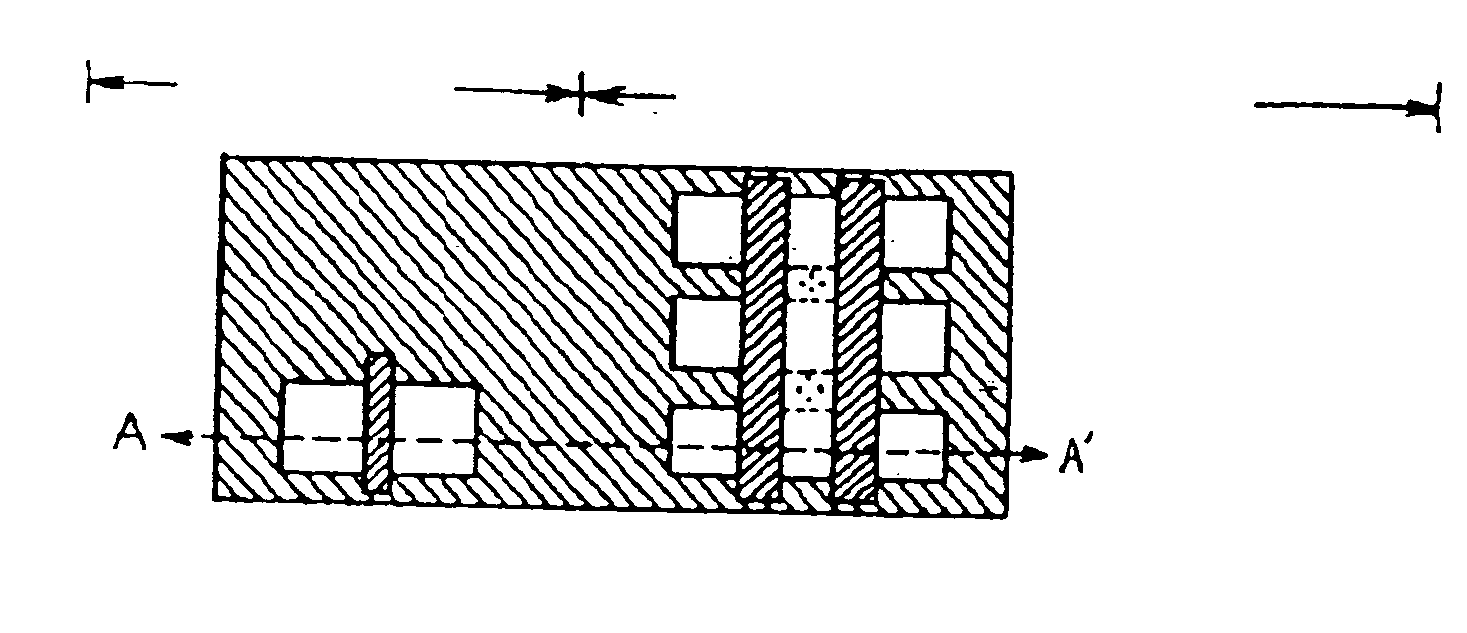
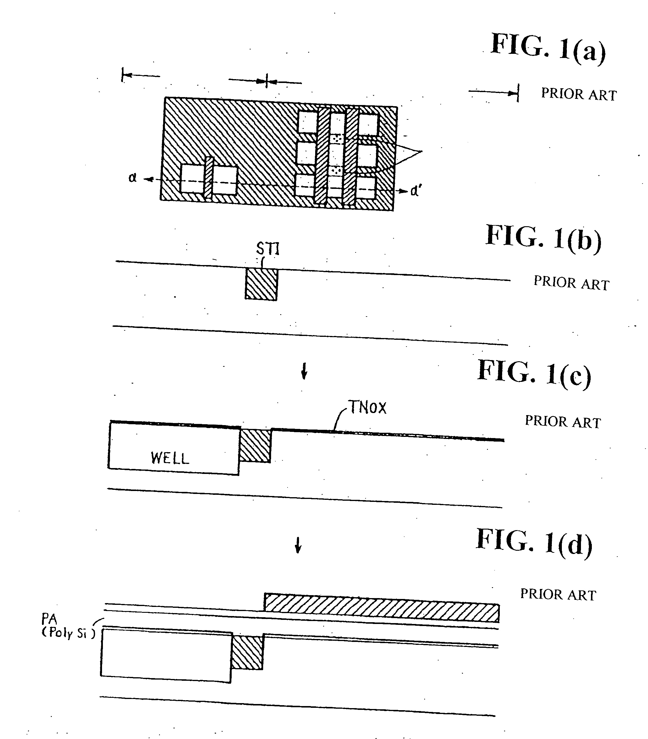
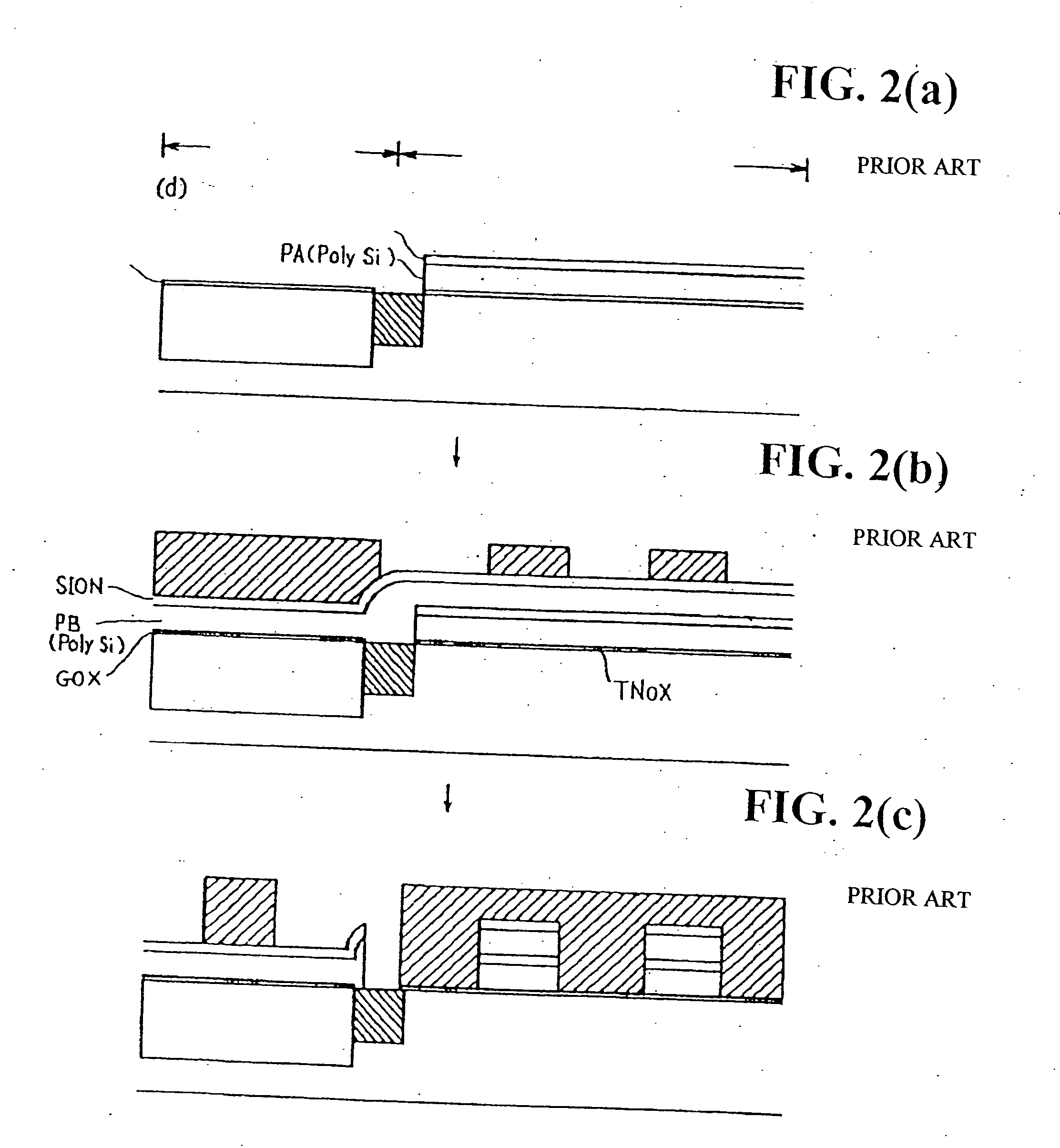
[0095]FIGS. 5 through 8 show cross-sectional views [A-A′ direction] of element regions configured in the first application embodiment of the present invention based on the damascene gate technique, and they show cross-sectional views of the element regions during the respective processes in proper order. FIGS. 9 through 13 show cross-sectional views [B-B′ direction] of a segment of the non-volatile memory cell region of the first application embodiment of the present invention based on the damascene gate technique from which an isolating insulation film has been removed (common source region), and they show cross-sectional views of the segment of the non-volatile memory cell region from which an isolating insulation film has been removed (common source region) during the respective processes in proper order. FIGS. 14 through 17 show cross-sectional views [C-C′ direction] of the word line direction of the non-volatile memory cell region of the first application embodiment of the pres...


PUM


Abstract

A non-volatile semiconductor memory device which simultaneously possesses a non-volatile memory cell region which possesses an isolating insulation film which has been formed selectively within a semiconductor substrate, which also possesses a first electroconductive film (floating gate electrode) via a first gate insulating film which has been formed on the semiconductor substrate surface, and which also possesses a metal film (control gate electrode) via a second gate insulating film which has been formed above said electroconductive film and a peripheral transistor region which possesses a metal film (gate electrode) via a third gate insulating film which has been formed above the semiconductor substrate surface.

Description

[0001] This application is a divisional of application Ser. No. 10 / 423,963, filed Apr. 28, 2003, which is a continuation of application Ser. No. 09 / 964,592, filed Sep. 28, 2001, which is now abandoned.FIELD OF THE INVENTION [0002] The present invention concerns a method for manufacturing a semiconductor device endowed with multiple functions. More specifically, it concerns a method for manufacturing a semiconductor device on which a non-volatile memory cell which consists of a double gate-type semiconductor element, etc. and a logic circuit unit which consists of a single gate-type semiconductor element have been heterogeneously mounted. BACKGROUND OF THE INVENTION [0003] Regarding semiconductor memory devices such as simple flash memories and EEPROMs (electrically re-writable non-volatile memory cells), one-chip products with added values which are endowed with the functions of peripheral circuits (e.g., logic device, etc.) have generated considerable demand in recent years in rela...

Claims


Application Information

Patent Timeline
Patent Type & Authority Applications(United States)
IPC IPC(8): H01L21/8238H01L21/316H01L21/28H01L21/8247H01L27/10H01L27/105H01L27/115H01L29/423H01L29/43H01L29/49H01L29/788H01L29/792
CPCH01L21/823842H01L21/823857H01L27/105H01L27/11546H01L27/11526H01L27/11543H01L27/115H01L29/66545H10B69/00H10B41/40H10B41/48H10B41/49H01L29/788H10B99/00
Inventor NAKAGAWA, SHIN-ICHIIIJIMA, MITSUTERU
Owner FUJITSU SEMICON LTD
Why Eureka
Try Eureka