Semiconductor device and manufacturing method thereof

a technology of semiconductor devices and semiconductors, applied in semiconductor devices, basic electric elements, electrical appliances, etc., can solve the problems of severe drawbacks, sub-threshold current increases, and short channel effects in transistors become severe, so as to achieve high performance in both transistors and prevent damage to the first gate insulating film

Active Publication Date: 2007-04-12
MICRON TECH INC
View PDF6 Cites 70 Cited by
  • Summary
  • Abstract
  • Description
  • Claims
  • Application Information

AI Technical Summary

Benefits of technology

[0039] According to the present invention, the first insulating film of the peripheral circuit region is protected by a protective film (conductive thin film) made from a non-doped silicon film or the like when the mask layer used to form the gate trench is removed after an impurity-doped first silicon film is formed in the gate trench. Damage to the first gate insulating film can therefore be prevented, and it is possible to embed an impurity-doped first silicon film i...

Problems solved by technology

However, short channel effects in a transistor become more severe as the gate length is shortened, and drawbacks occur whereby sub-threshold current increases.
When the substrate impurity concentration is increased in order to minimize this effect, deterioration of the refresh characteristics in the DRAM is a severe drawback because of increased junction leakage.
However, such drawbacks as the following occur when transistors having the two structures described above are used jointly in a single semiconductor device.
However, in this first conventional method, when ion implantation is performed according to the thickness (depth) of the silicon film 204 on...

Method used


Image

  • Semiconductor device and manufacturing method thereof
  • Semiconductor device and manufacturing method thereof
  • Semiconductor device and manufacturing method thereof

Examples


Embodiment Construction

[0069] Preferred embodiments of the present invention will now be explained in detail with reference to the drawings.

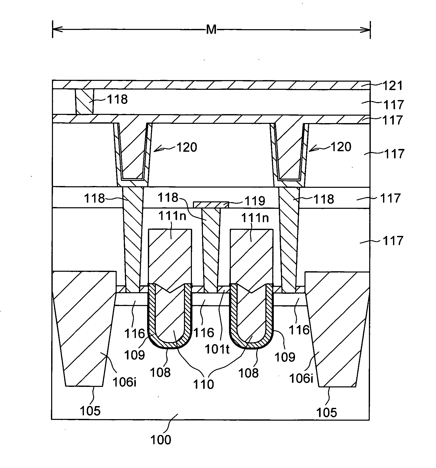
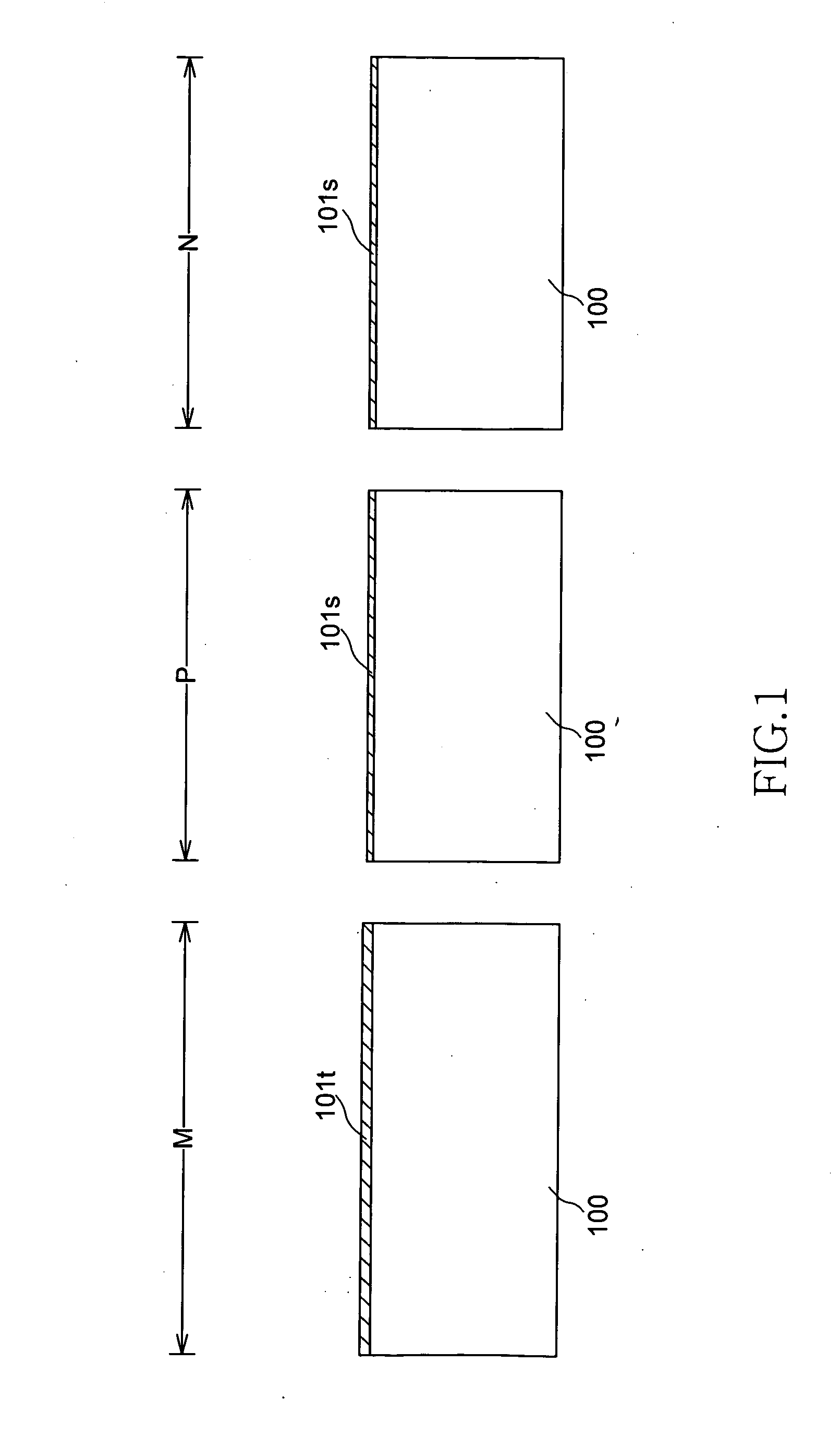
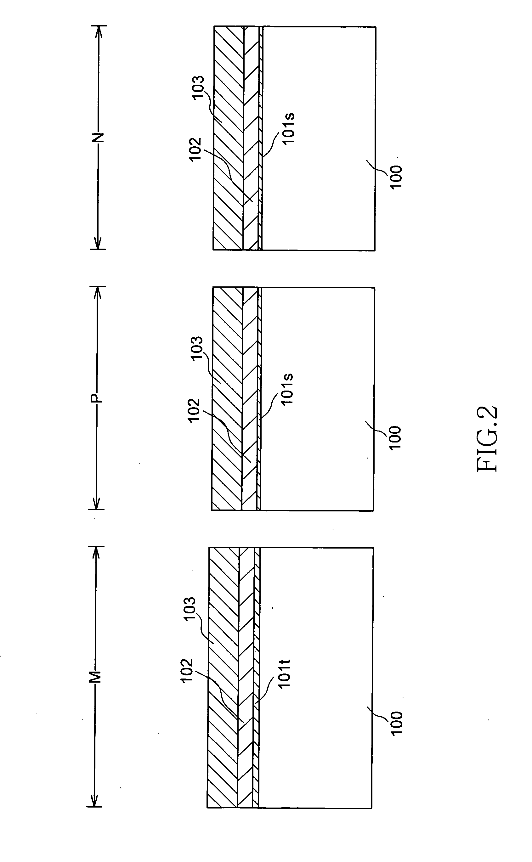
[0070]FIGS. 1 through 20 are schematic views showing the process for manufacturing a semiconductor device that has a trench-gate transistor and a dual-gate-structured transistor according to an embodiment of the present invention. In FIGS. 1 through 20, “region M” indicates the memory cell region in which the trench-gate transistor is formed, and “region P” and “region N” are provided to the peripheral circuit region, wherein “region P” is a region (also referred to as a P-type peripheral circuit region) in which a planar P-channel transistor provided with a gate electrode that includes P-type polycrystalline silicon is formed, and “region N” is a region (also referred to as an N-type peripheral circuit region) in which a planar N-channel transistor provided with a gate electrode that includes N-type polycrystalline silicon is formed.

[0071] First, a thin oxide film ...


PUM


Abstract

Gate trenches 108 are formed in a memory cell region M using a silicon nitride film 103 as a mask in a state in which the semiconductor substrate 100 in a P-type peripheral circuit region P and an N-type peripheral circuit region N is covered by a gate insulating film 101s, a protective film 102, and the silicon nitride film 103. A gate insulating film 109 is then formed on the inner walls of the gate trenches 108, and a silicon film 110 that includes an N-type impurity is embedded in the gate trenches 108. The silicon nitride film 103 is then removed, and a non-doped silicon film is formed on the entire surface, after which a P-type impurity is introduced into the non-doped silicon film on region P, and an N-type impurity is introduced into the non-doped silicon film on regions M and N.

Description

TECHNICAL FIELD [0001] The present invention relates to a semiconductor device and to a method for manufacturing the same, and particularly relates to a semiconductor device and a method for manufacturing a semiconductor device having both a trench-gate transistor and a dual-gate transistor. BACKGROUND OF THE INVENTION [0002] The recent miniaturization of DRAM (Dynamic Random Access Memory) cells has been accompanied by the necessity of shortening the gate length of memory cell transistors. However, short channel effects in a transistor become more severe as the gate length is shortened, and drawbacks occur whereby sub-threshold current increases. When the substrate impurity concentration is increased in order to minimize this effect, deterioration of the refresh characteristics in the DRAM is a severe drawback because of increased junction leakage. [0003] A so-called trench-gate transistor (also referred to as a recess-channel transistor) in which a gate electrode is embedded in a ...

Claims


Application Information

Patent Timeline
IPC IPC(8): H01L21/8242H01L21/76
CPCH01L21/823437H01L29/66621H10B12/05H10B12/053H10B12/09
Inventor SHIRATAKE, SHIGERU
Owner MICRON TECH INC
Why Eureka
Try Eureka