Semiconductor integrated circuit device and a manufacturing method for the same

a technology of integrated circuit device and manufacturing method, which is applied in the direction of semiconductor devices, basic electric elements, electrical equipment, etc., can solve the problems of reducing the esd immunity, the esd immunity falls below the standard, and the element is destroyed, so as to improve the esd immunity and the element's destruction resistance, reduce the drain resistance, and prevent the effect of thermal destruction of silicon

Inactive Publication Date: 2007-04-19
ABLIC INC
View PDF3 Cites 5 Cited by
  • Summary
  • Abstract
  • Description
  • Claims
  • Application Information

AI Technical Summary

Benefits of technology

[0080] As described above, according to the manufacturing method for a power management semiconductor device or an analog semiconductor device both including a CMOS transistor, disposition and connection of an extension region on and above a part of a silicon surface of a low impurity concentration drain region in a MOS transistor helps to reduce the drain resistance during normal circuit operation, and to advance thermal diffusion in the low impurity concentration drain region during high current operation or at the time of an ESD surge input, preventing thermal destruction of silicon by suppressing the temperature rising, thereby improving an ESD immunity and a destruction resistance of the element. Accordingly, increase in the freedom in setting the concentration for the low impurity concentration drain region leads to an easy implementation of transistor characteristics as desired.

Problems solved by technology

According to the semiconductor device manufactured according to the conventional methods described above, formation of a drain region at a lower concentration of impurity for the purpose of ensuring high junction breakdown voltage, surface breakdown voltage, snap-back voltage, or a low impact ionization rate, results in a reduction in an ESD immunity, which may eventually lead to a case where the ESD immunity falls below standards.
There also occurs a phenomenon in which a large amount of drain current causes a self-heating in the low impurity concentration region, particularly in a portion having a high resistance, causing a current concentration thereto, which leads to destruction of the element.
That is, inconsistency between important characteristics of a transistor and the ESD immunity sometimes comes out, and leads to a problem in that characteristics and standards cannot be satisfied together without increase in transistor size to face an increase in cost along with the increase in chip area.
Also, wiring metal in the contact region in general is not excellent in its coverage, which is about 20% of the wiring metal thickness in a flat area.
Such low coverage is a main reason for limiting current density, which accordingly makes it difficult to pass a large amount of current without increase in a contact area.

Method used


Image

  • Semiconductor integrated circuit device and a manufacturing method for the same
  • Semiconductor integrated circuit device and a manufacturing method for the same
  • Semiconductor integrated circuit device and a manufacturing method for the same

Examples


first embodiment

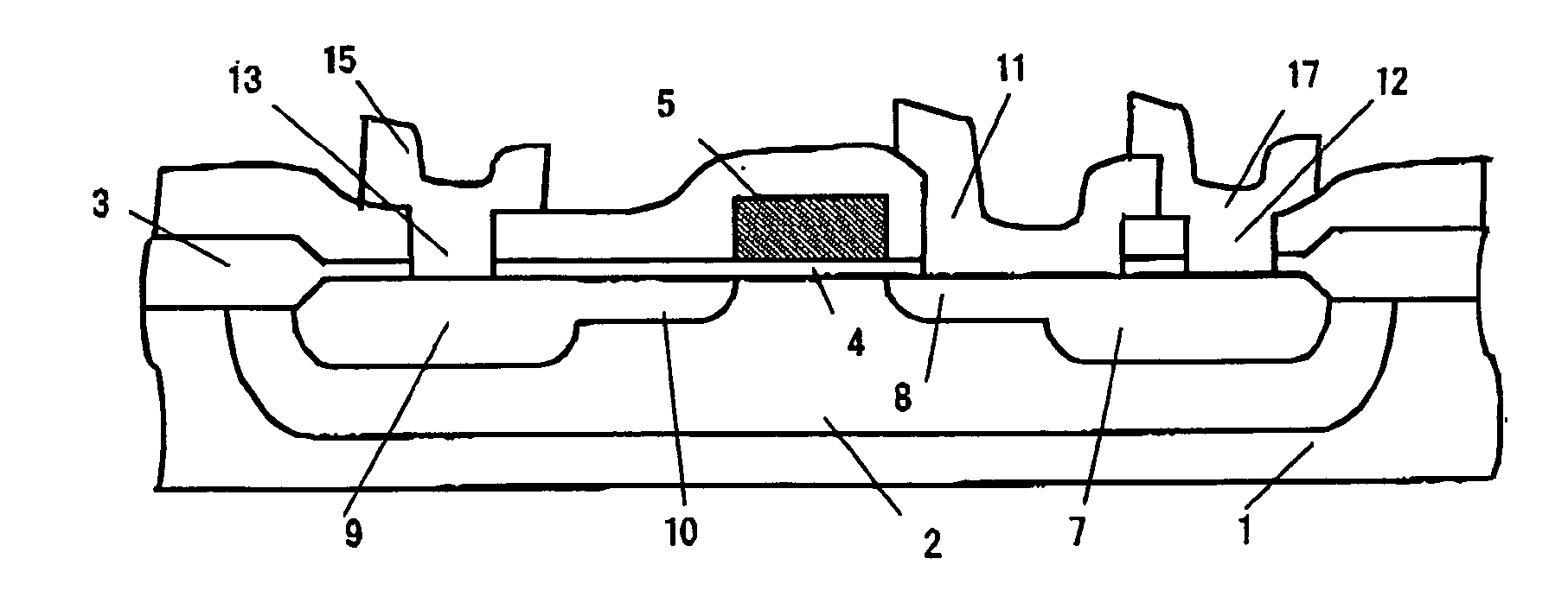
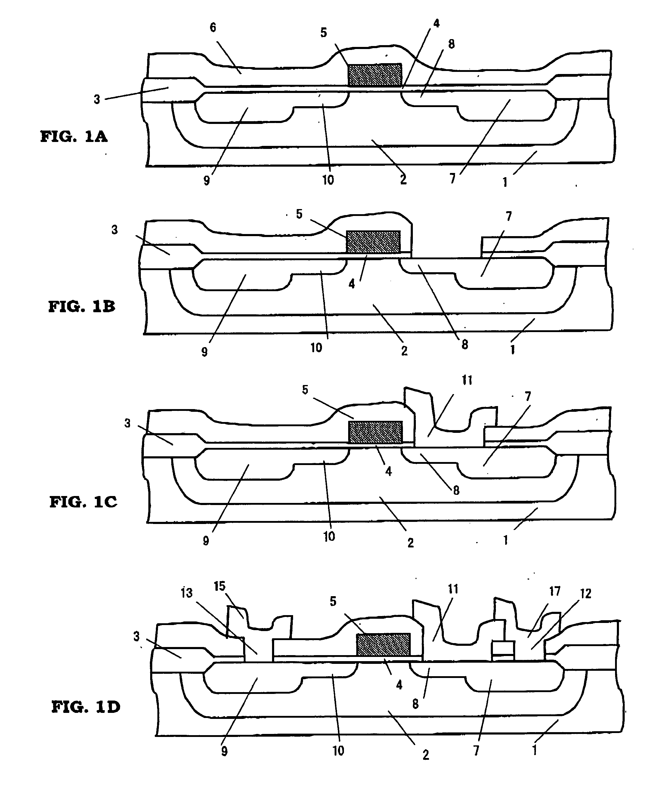
[0092]FIGS. 1A to 1D are schematic cross-sectional diagrams showing sequential process steps according to a manufacturing method for a semiconductor device of the present invention.

[0093] In FIG. 1A, a P-type semiconductor substrate 1, for example, doped with boron at an impurity concentration to attain a resistivity of 20 Ωcm to 30 Ωcm, is subjected to, for example, ion implantation of boron at a dose of 1×10¹¹ atoms / cm2 to 1×10¹³ atoms / cm2 and to annealing at 1,000 to 1,200° C. for several hours to ten-odd hours, to form a diffusion layer or a P-type well 2. Here, an explanation is given to process steps for forming a P-type well on a P-type semiconductor substrate, while a P-type well may also be formed on an N-type semiconductor substrate in a similar manner. The substrate can have either conductivity type, which is irrelevant to the gist of the present invention.

[0094] Then, a field insulating film 3, for example, a thermal oxide film with a thickness of several thousands Å to...

second embodiment

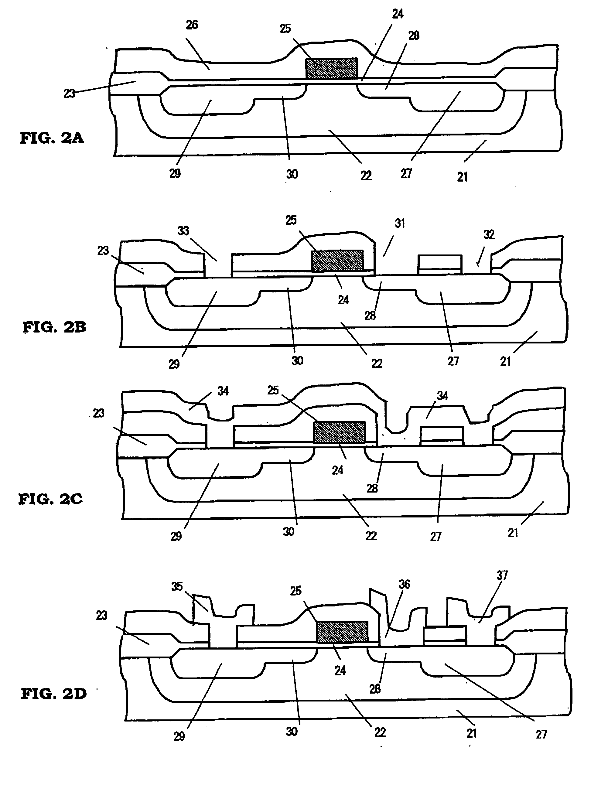
[0101]FIGS. 2A to 2D are schematic cross-sectional diagrams showing sequential process steps according to a manufacturing method for a semiconductor device of the present invention.

[0102] In FIG. 2A, a P-type semiconductor substrate 21, for example, doped with boron at an impurity concentration to attain a resistivity of 20 Ωcm to 30 Ωm, is subjected to, for example, ion implantation of boron at a dose of 1×10¹¹ atoms / cm2 to 1×10¹³ atoms / cm2 and to annealing at 1,000 to 1,200° C. for several hours to ten-odd hours, to form a diffusion layer or a F-type well 22. Here, an explanation is given on process steps for forming a P-type well on a P-type semiconductor substrate, while a F-type well may also be formed on an N-type semiconductor substrate in a similar manner. The substrate can have either conductivity type, which is irrelevant to the gist of the present invention.

[0103] Then, a field insulating film 23, for example, a thermal oxide film with a thickness of several thousands Å ...

third embodiment

[0109]FIGS. 3A to 3D are schematic cross-sectional diagrams showing sequential process steps according to a manufacturing method for a semiconductor device of the present invention.

[0110] As shown in FIG. 3A, a P-type semiconductor substrate 41, for example, doped with boron at an impurity concentration to attain a resistivity of 20 Ωcm to 30 Ωcm, is subjected to, for example, ion implantation of boron at a dose of 1×10¹¹ atoms / cm2 to 1×10¹³ atoms / cm2 and to annealing at 1,000 to 1,200° C. for several hours to ten-odd hours, to form a diffusion layer or a P-type well 42. Here, an explanation is given on process steps for forming a P-type well on a P-type semiconductor substrate, while a P-type well may also be formed on an N-type semiconductor substrate in a similar manner. The substrate can have either conductivity type, which is irrelevant to the gist of the present invention.

[0111] Then, a field insulating film 43, for example, a thermal oxide film with a thickness of several th...


PUM


Abstract

Provided is a manufacturing method for a power management semiconductor device or an analog semiconductor device both including a CMOS. According to the method, a substance having high thermal conductivity is additionally provided above a semiconductor region constituting a low impurity concentration drain region so as to expand the drain region, which contributes to a promotion of thermal conductivity (or thermal emission) in the drain region during a surge input and leads to suppression of local temperature increase, to thereby prevent thermal destruction. Therefore, it is possible to manufacture a power management semiconductor device or an analog semiconductor device with the extended possibility of transistor design.

Description

BACKGROUND OF THE INVENTION [0001] 1. Field of the Invention [0002] The present invention relates to a semiconductor integrated circuit device and a manufacturing method for the same in which low voltage operation with low power consumption and high driving capacity is required. In particular, the present invention relates to a manufacturing method for a power management semiconductor device such as a voltage detector (hereinafter, referred to as VD), a voltage regulator (hereinafter, referred to as VR), or a switching regulator (hereinafter, referred to as SWR). [0003] 2. Description of the Related Art [0004] A conventional technology is explained with reference to FIGS. 8A to 8C. FIGS. 8A to 8C are schematic cross-sectional views showing sequential process steps of a manufacturing method for a semiconductor device according to a conventional technology. An NMOS transistor having an offset type LDD structure is shown as an example. [0005] AS shown in FIG. 8A, a P-type semiconductor...

Claims


Application Information

Patent Timeline
Patent Type & Authority Applications(United States)
IPC IPC(8): H01L29/76
CPCH01L29/402H01L29/405H01L29/41725H01L29/41775H01L29/4983H01L29/7834H01L29/7835H01L21/18
Inventor SAITOH, NAOTOKITAJIMA, YUICHIRO
Owner ABLIC INC
Why Eureka
Try Eureka