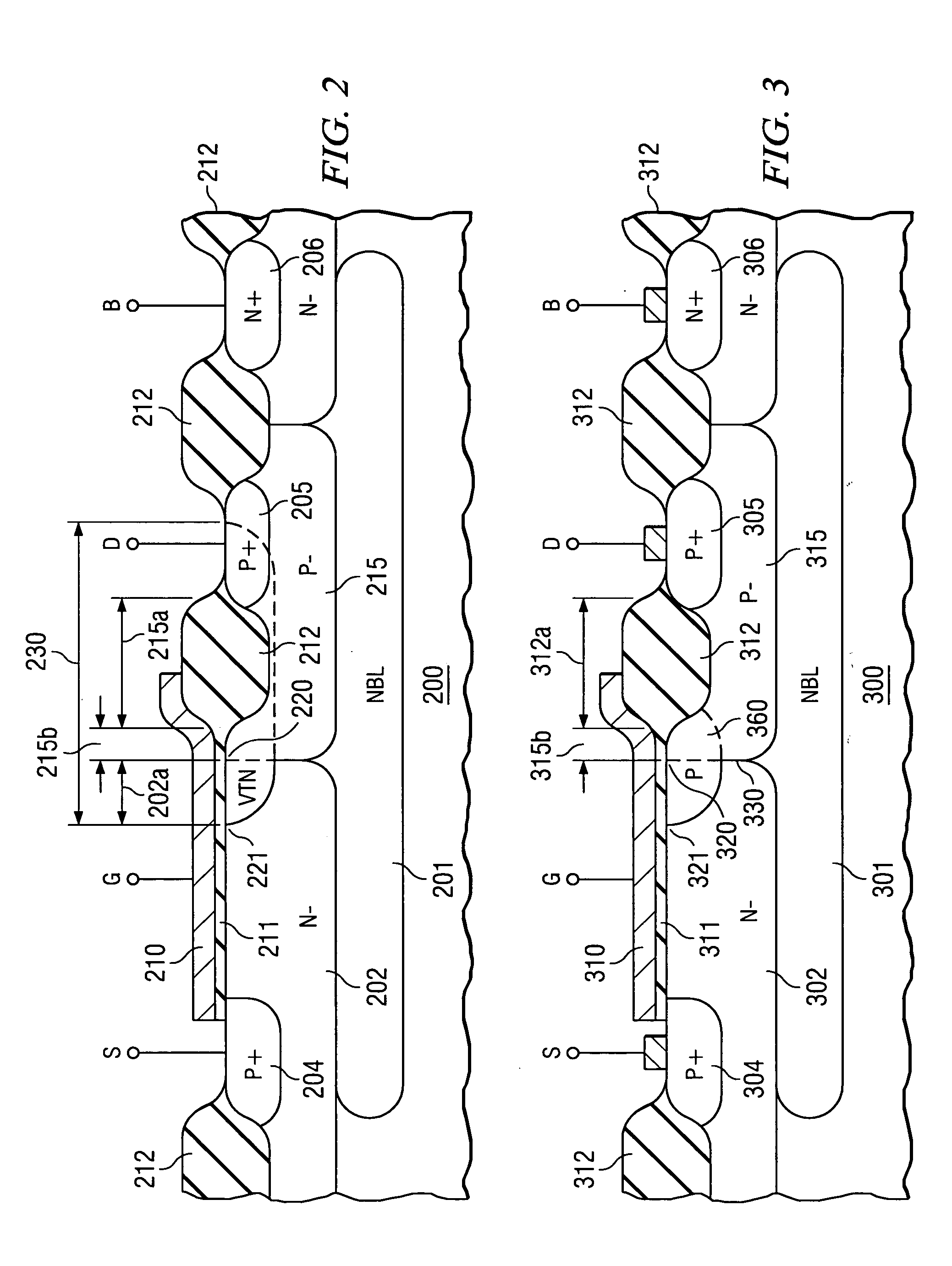
[0026] Another technical
advantage of the invention becomes evident from the fact that the extent of length 215b can be considered as an effect of process tolerance, causing some uncertainty about the size of the
high resistance region of the p-well 215. The VT adjust
implant, however, strongly reduces the resistance of the process tolerance region 215b and thus renders the
high resistance region in p-well 215 exact, eliminating the resistance uncertainty. The drain extension for drain 305 is now exactly the length 215a of the
field oxide, a fact which amount to a smaller size of the MOS device. This technical
advantage of the invention strongly supports the general
miniaturization trend of the
semiconductor technology.
[0027] While the device illustrated in FIG. 2 is a pMOS device, other embodiments of the invention employ nMOS devices, since the invention is equally applicable to pMOS and nMOS devices. One of ordinary skill in the art should realize, based on the instant recitations, which dopants and
doping levels to use to convert the invention so as to be applicable to nMOS type devices. The result of the additional n-type
implant is a lower
drain resistance of the nMOS transistor and thus a higher drain current, while the transistor breakdown
voltage remains high.
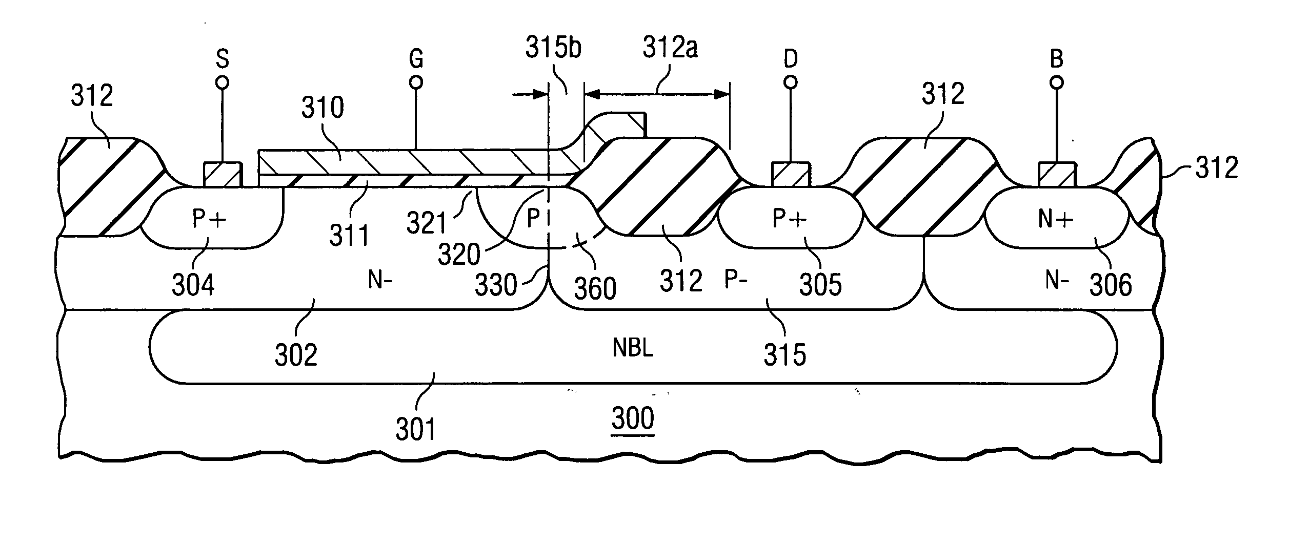
[0028]FIG. 3 depicts in a
schematic cross section the structure resulting from of the additional
threshold voltage ion implant. As in FIG. 2, the example chosen refers to a one-sided p-channel drain-extended pMOS transistor in a p-type substrate 300 with an n-type buried layer 301; other embodiments of the invention use an analogous nMOS transistor (see FIGS. 9 and 10). Well region 302 is an n-doped well, over which
gate oxide 311 is located. The thickness of
gate oxide 311 is preferably 20 nm or less. Well region 315 is a p-doped well surrounding p+ drain 305, extending under the
field oxide layer 312. The length 312a of the
field oxide 312 determines exactly the drain extension and thus the breakdown voltage of the transistor and the resistance of the drain extension. The drain extension allows transistors with a breakdown voltage of about 30 V (for higher voltages see FIG. 8). The additional length 315b of the p-well 315 is heavily doped by the additional
boron implant according to the invention and thus helps to reduce the overall drain resistance. The n-well is contacted by
body contact 306. P+ source 304 is located in n-well 302. Well 302 and well 315 form a junction, which intersects with the
gate oxide 311 at location 321.
[0029] Another embodiment of the present invention is a method for reducing the drain resistance of a drain-extended MOS transistor in a semiconductor
wafer, while maintaining a high transistor breakdown voltage. One such method 400 is illustrated and described in FIG. 4, another method 600 is illustrated and described in FIG. 6. Although the exemplary methods 400 and 600 are illustrated and described as a series of acts or events, it will be appreciated that the present invention is not limited by the illustrated ordering of such acts or events, as some acts or events may occur in different orders and / or concurrently with other acts or events apart from those illustrated and described herein, in accordance with the invention. In addition, not all illustrated steps may be required to implement a methodology in accordance with the present invention. Moreover it will be appreciated that the method according to the present invention may be implemented in the fabrication of the semiconductor devices illustrated and described herein as well as in producing other devices not illustrated or described.
[0030] Beginning at step 401 in FIG. 4, the method 400 comprises providing at step 402 a well of a first conductivity type, operable as the extension of the transistor drain of the first conductivity type and covered by a first insulator having a first thickness. The first insulator thickness range is preferably from about 450 to 600 nm. Further provided is a well of the opposite conductivity type, intended to contain the transistor source of the first conductivity type and covered by a second insulator, which is thinner than the first insulator. The thickness of the second insulator is preferably in the range from 5 to 50 nm. The first and second wells form a junction that terminates at the second insulator.
[0031] At step 403, a
photoresist layer is deposited over the MOS transistor. This
photoresist layer is patterned at step 404 by opening a window, which extends laterally from the drain region to a distance in the second well slightly beyond the termination of the well junction at the second insulator.

