

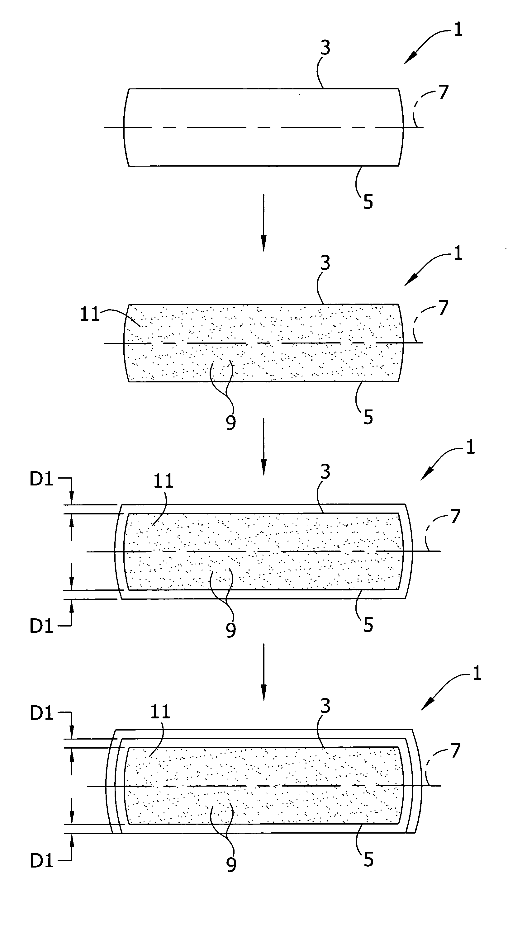
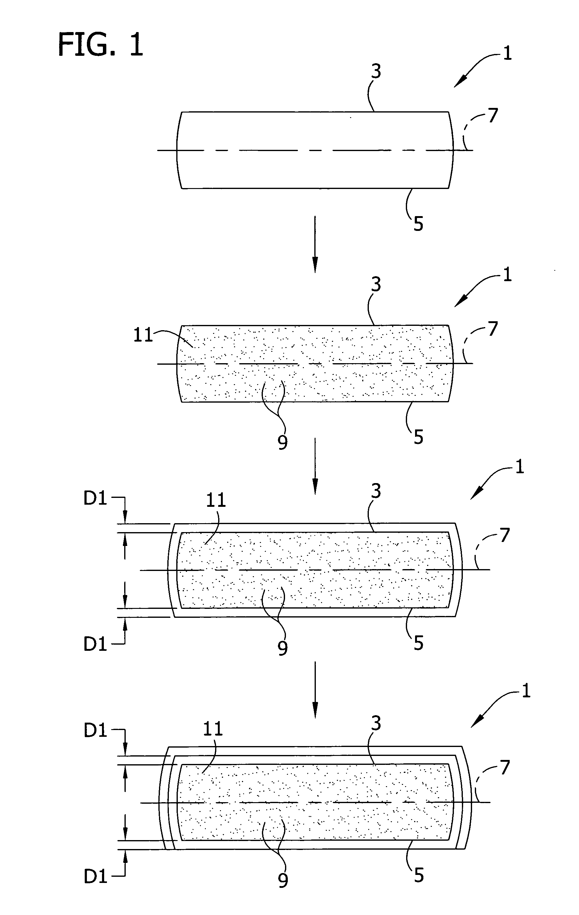
Arsenic and phosphorus doped silicon wafer substrates having intrinsic gettering
a technology of arsenic and phosphorus, which is applied in the field of silicon wafer preparation, can solve the problems of affecting the operation of the device, contaminating molten silicon with various impurities, and precipitating harmful or beneficial effects, and achieves greater wafer-to-wafer uniformity and low resistivity
- Summary
- Abstract
- Description
- Claims
- Application Information
AI Technical Summary
Benefits of technology
Problems solved by technology
Method used
Image

Examples
example
[0048] Red phosphorus doped silicon single crystals were pulled by the Czochralski method, sliced and polished to form silicon wafers. The initial oxygen concentration of each wafer was from about 12 PPMA to about 18 PPMA, and the resistivity was from about 1.2 mΩ-cm to about 1.7 mΩ-cm. The wafers were then subjected to rapid thermal annealing in nitrogen, rapidly cooled, and subjected to oxygen precipitate stabilization and growth. The temperature of the rapid thermal anneal was varied as shown in TABLE I, but all samples were annealed for 15 seconds. The samples were cooled at 60° C. / sec. Oxygen precipitate formation and stabilization occurred at 800° C. temperature for 4 hours, followed by 1000° C. for 16 hours. The average concentration and peak concentration of oxygen precipitates were measured at the center, at half the radius, and at the edge of each wafer. It was observed that for all samples the peak concentration occurred near the wafer surface. The results are depicted in...
PUM
 Abstract
Description
Claims
Application Information