

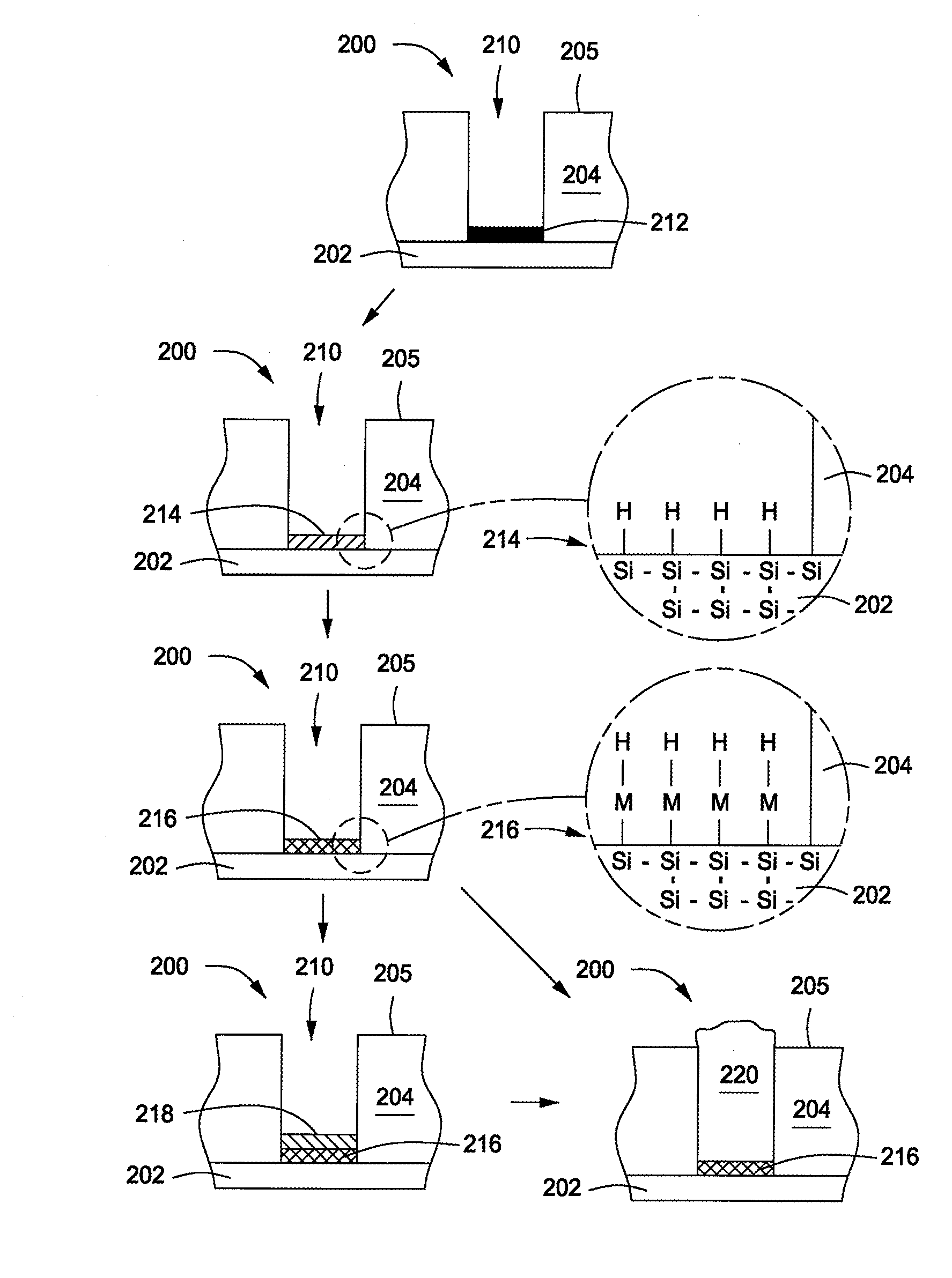
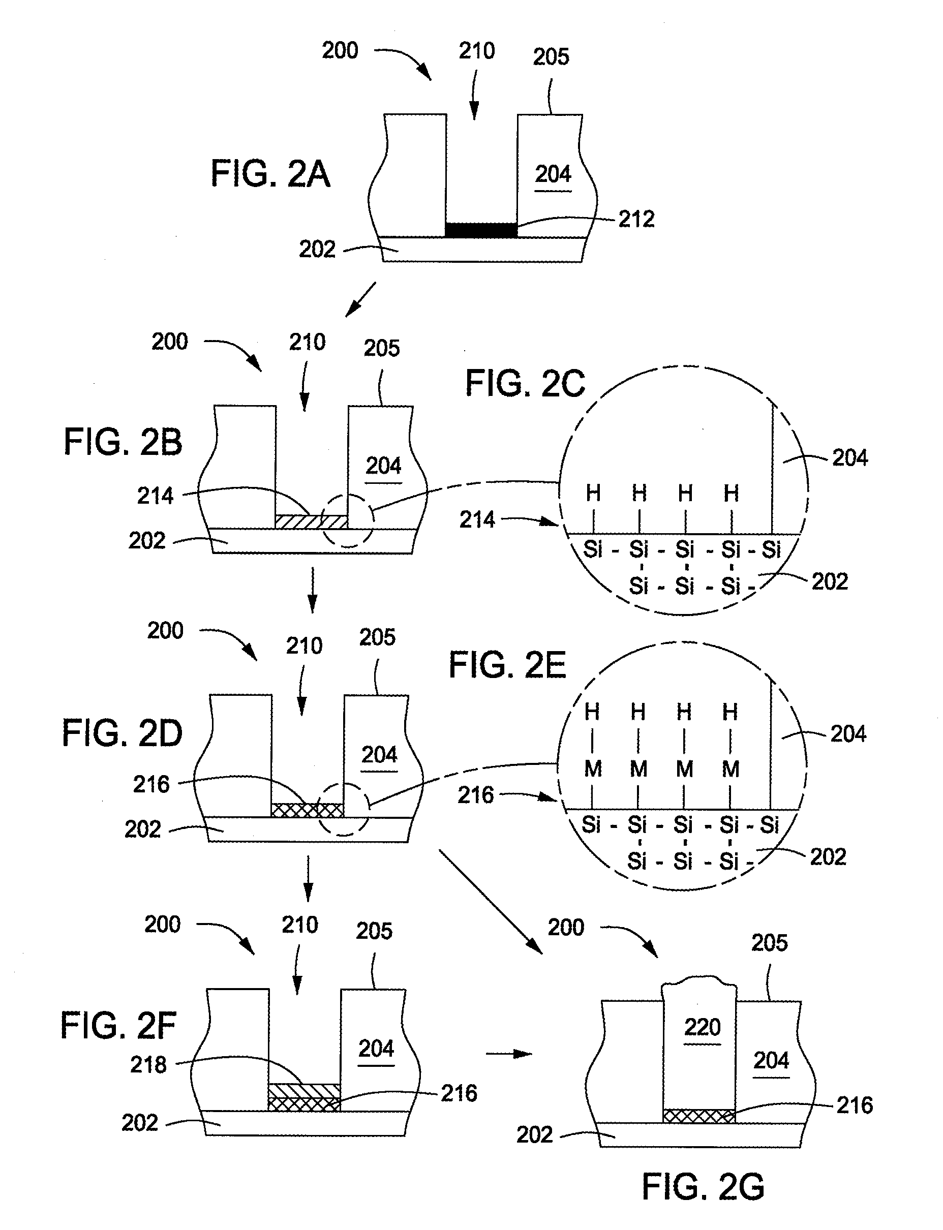
Method of selectively depositing a thin film material at a semiconductor interface
a thin film material and semiconductor technology, applied in the direction of detergent compositions, inorganic non-surface active detergent compositions, etc., can solve the problems of affecting the device yield of the fabricated substrate, the displacement of voids from one layer to the next, and the defect of contact plugs in the vapor deposition process
- Summary
- Abstract
- Description
- Claims
- Application Information
AI Technical Summary
Benefits of technology
Problems solved by technology
Method used
Image

Examples
example 1
DEA-HF Concentrate
[0100] Diethanolamine (DEA) 99.5% (1 mole, 105.1 g) is heated to its melting point and dissolved in minimal ultra pure water to form a concentrated solution within a 500 mL vessel. To the vessel, 200 mL of diluted 10% wt. hydrofluoric acid, or 1 mole of HF is added slowly enough to prevent excessive heating of the solution. The pH value of the solution is adjusted to a desired pH range with the direct addition of 48% wt. HF or 33% wt. tetramethylammonium hydroxide (TMAH), or a non-fluoride containing acid such as sulfuric acid (H2SO4). The solution is diluted with pure water to a volume of 500 mL. The DEA-HF concentrate has a DEA concentration of about 2 M.
example 1.1
DEA-HF Concentrate of pH 6-7
[0101] A 500 mL of DEA-HF concentrate (about 500 g) having a pH value within a range from about 6 to about 7 contains about 105 g of DEA (about 20% wt.), about 20 g of HF (about 5% wt.), and about 375 g (about 75% wt.) of water.
example 1.2
DEA-HF Concentrate of pH 4-4.5
[0102] A 500 mL of DEA-HF concentrate (about 500 g) having a pH value within a range from about 4 to about 4.5 contains about 105 g of DEA (about 20% wt.), about 35 g of HF (about 7% wt.), and about 365 g (about 73% wt.) of water. The pH value is adjusted to the point of zero charge (PZC) of silicon, which is also within a range from about 4 to about 4.5.
PUM
| Property | Measurement | Unit |
|---|---|---|
| viscosity | aaaaa | aaaaa |
| viscosity | aaaaa | aaaaa |
| viscosity | aaaaa | aaaaa |
Abstract
Description
Claims
Application Information