This helps you quickly interpret patents by identifying the three key elements:
Problems solved by technology
Method used
Benefits of technology
Benefits of technology
[0012] In view of the foregoing, it is an object of the present invention to provide a light-emitting element capable of being increased its thickness and operating at low driving voltage by a novel means different from a light-emitting element using a material serving as a ligand in accordance with the prior art. It is more specific object of the present invention to provide a light-emitting element that consumes low power and emits light with good color purity. It is still more specific object of the present invention to provide a light-emitting element that consumes low power and is manufactured in high yields.
[0024] Despite of using sputtering for forming the cathode in the light-emitting element according to the present invention, a light-emitting element having good characteristics and being suffered from little damage due to the sputtering can be obtained. Therefore, a cathode can be formed by using a conductive material that is transparent to visible light such as ITO (IndiumTinOxide) that is mainly formed by sputtering. In the case of using such the transparent electrode made from a conductive material transparent to visible light, a light-emitting element that can emit light from a cathode can be obtained.
[0025] By a novel means according to the present invention different from the conventional light-emitting element using a material serving as a ligand, a light-emitting element capable of readily being increased its thickness and operating at low driving voltage can be obtained. Accordingly, a light-emitting element that consumes low power and emits light with good color purity can be obtained. Simultaneously, a light-emitting element that consumes low power and is manufactured in high yields can be obtained.
[0026] By using the foregoing light-emitting element for manufacturing a light-emitting device, a light-emitting device that can emit light with good color purity and consumes low power can be manufactured in high yields.
Problems solved by technology
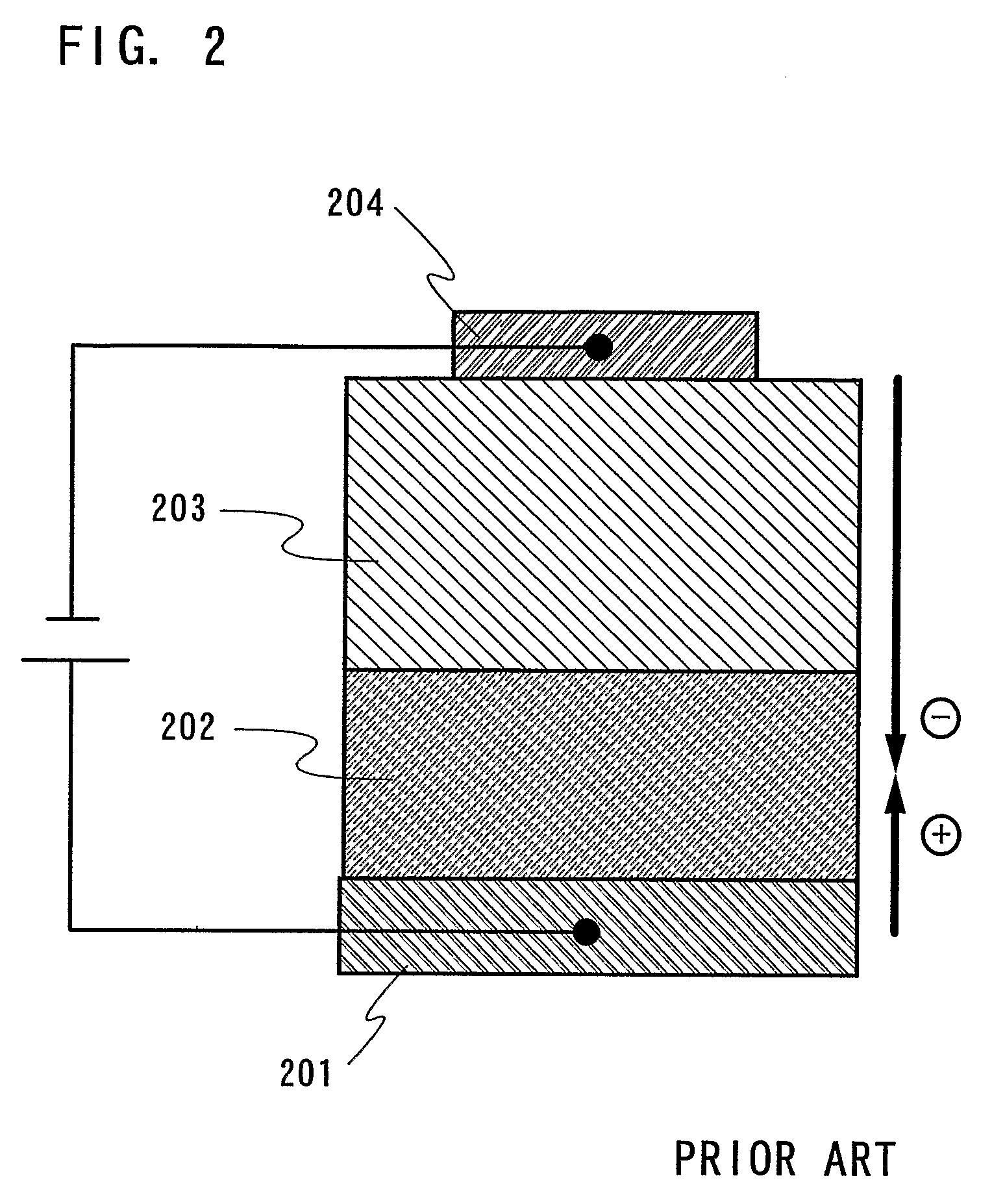
Therefore, the technique with respect to an electron injecting layer disclosed in the Unexamined Patent Publications Nos. 10-270171 and 2001-102175 has a problem that even if the thickness of the electron injecting layer is increased to improve a manufacturing yield, or to control an emission spectrum so that color purity is improved, power consumption is increased unless an organic compound serving as a ligand is selected to use.
Method used
Image
Click on the blue label to locate the original text in one second.
Reading with bidirectional positioning of images and text.
Examples
embodiment 1
[0053] A light-emitting element according to the present invention is explained in Embodiment 1 with reference to FIGS. 3A to 3C.
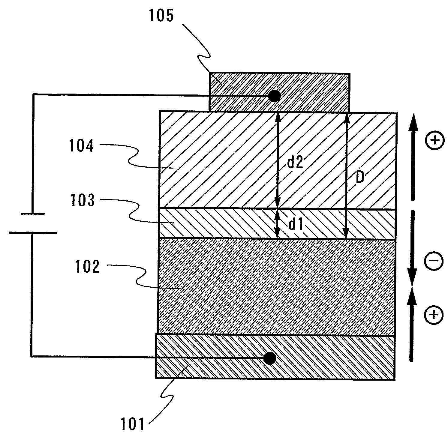
[0054] As illustrated in FIGS. 3A to 3C, a light-emitting element has a configuration composed of an anode 301 formed over a substrate 300, a first layer containing a light-emitting material 302 formed over the anode 301, a second layer 303 formed over the first layer 302, a third layer 304 formed over the second layer 303, and a cathode 305 formed over the third layer 304.
[0055] As a material for the substrate 300, any substrate as long as it is used in the conventional light-emitting element can be used. For example, a glass substrate, a quartz substrate, a transparent plastic substrate, or a substrate having flexibility can be used.
[0056] As an anode material for forming the anode 301, metal having a large work function (at least 4.0 eV), alloys, compounds having electrical conduction properties, and mixture of these materials are preferably used. As...
embodiment 2
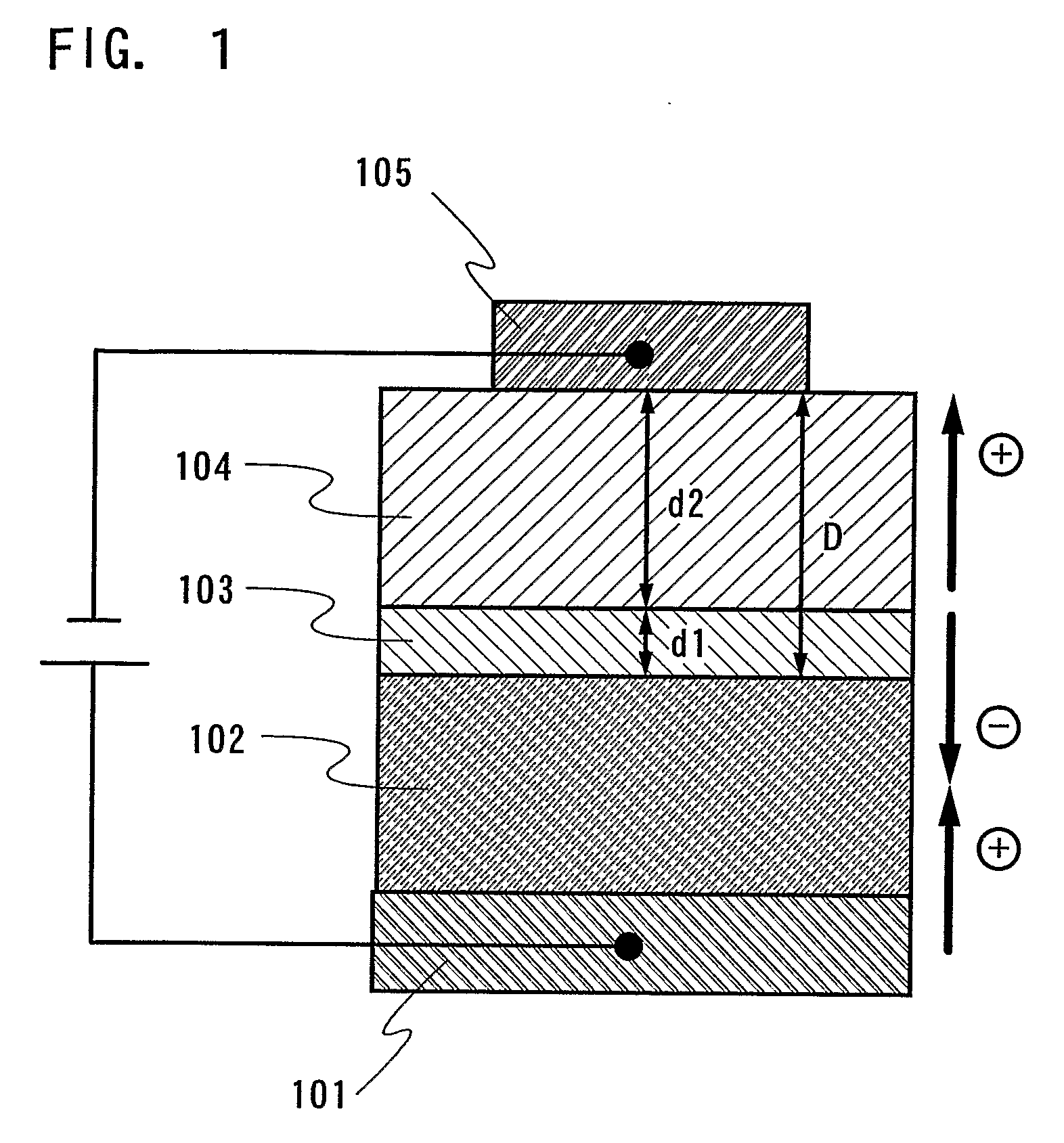
[0073] A configuration of a light-emitting element according to the present invention is explained with reference to FIGS. 4A to 4C in Embodiment 2.
[0074] A substrate 400, an anode 401, a first layer 402, a second layer 403, a third layer 404, and a cathode 405 can be formed by the same materials and the same processes explained in Embodiment 1, and are explained in no more details.
[0075] As illustrated in FIGS. 4A to 4C, a light-emitting element has a configuration composed of a cathode 405 formed over the substrate 400, the third layer 404 formed over the cathode 405, the second layer 403 formed over the third layer 404, the first layer 402 containing a light-emitting material formed over the second layer 403, and the anode 401 formed over the first layer 402.
[0076] A light-emitting element according to the invention has the structure that light generated by recombination of carries within the first layer containing the light-emitting material is emitted from either the anode 4...
embodiment 3
[0081] In this embodiment, a light-emitting element is manufactured over a substrate 500 such as a glass, quartz, metal, bulk semiconductor, transparent plastic, or flexible substrate. A passive light-emitting device can be manufactured by a plurality of such the light-emitting elements over one substrate. A light-emitting element may be manufactured to be in contact with a thin film transistor (TFT) array as shown in FIG. 5 instead of manufacturing the light-emitting element over the substrate such as a glass, quartz, transparent plastic, or flexible substrate. Here, reference numeral 511 denotes a TFT; 512, a TFT; and 513, a light-emitting element according to the present invention. The light-emitting element 513 is composed of an anode 514, first, second, and third layers 515, and a cathode 516; and is connected electrically to the TFT 511 via a wiring 517. Thus, an active matrix light-emitting device that controls driving of a light-emitting element by a TFT can be manufactured....
PUM
Abstract
In the present invention, a light-emitting element operating at low driving voltage, consuming low power, emitting light with good color purity and manufactured in high yields can be obtained. A light-emitting element is disclosed with a configuration composed of a fist layer containing a light-emitting material, a second layer, a third layer are formed sequentially over an anode to be interposed between the anode and a cathode in such a way that the third layer is formed to be in contact with the cathode. The second layer is made from n-type semiconductor, a mixture including that, or a mixture of an organic compound having a carrier transporting property and a material having a high electron donor property. The third layer is made from p-type semiconductor, a mixture including that, or a mixture of an organic compound having a carrier transporting property and a material having a high electronacceptor property.
Description
TECHNICAL FIELD [0001] The present invention relates to a layered structure of a light-emitting element that has a layer containing a light-emitting material between an anode and a cathode and that can emit light upon being applied with an electric field. BACKGROUND ART [0002] As examples of a photoelectronic device using an organic semiconductor material as a functional organic material, a light-emitting element, solar battery, and the like can be nominated. These are devices utilizing an electrical property (carrier transporting property) or an optical property (light absorption or light-emitting property) of the organic semiconductor material. Among others, a light-emitting element has achieved remarkable development. [0003] A light-emitting element comprises a pair of electrodes (anode and cathode) and a layer containing a light-emitting material interposed between the pair of electrodes. The emission mechanism is as follows. Upon applying voltage through the pair of electrodes,...
Claims
Application Information
Patent Timeline
Application Date:The date an application was filed.
Publication Date:The date a patent or application was officially published.
First Publication Date:The earliest publication date of a patent with the same application number.
Issue Date:Publication date of the patent grant document.
PCT Entry Date:The Entry date of PCT National Phase.
Estimated Expiry Date:The statutory expiry date of a patent right according to the Patent Law, and it is the longest term of protection that the patent right can achieve without the termination of the patent right due to other reasons(Term extension factor has been taken into account ).
Invalid Date:Actual expiry date is based on effective date or publication date of legal transaction data of invalid patent.

