Amorphous transparent conductive film, sputtering target as its raw material, amorphous transparent electrode substrate, process for producing the same and color filter for liquid crystal display

a technology of conductive film and amorphous transparent electrode, which is applied in the direction of conductors, instruments, non-linear optics, etc., can solve the problems of liquid crystal-driving transparent electrode, transparent electrode is easily cracked or peeled, and the thermal stability and moisture resistance of the above-mentioned ito film is relatively low

Inactive Publication Date: 2007-05-24
IDEMITSU KOSAN CO LTD
View PDF4 Cites 29 Cited by
  • Summary
  • Abstract
  • Description
  • Claims
  • Application Information

AI Technical Summary

Benefits of technology

[0083] The following describes a second group invention for attaining the above-mentioned second object mainly. This second group invention will be described in detail by way of a second embodiment that will be described later. The transparent electrode of the second group is substantially equal to the amorphous transparent electroconductive film of the first group. In the second group invention, the amorphous transparent electroconductive film is used as an electrode; thus, attention is paid to the function thereof, whereby the film is called the transparent electrode.
[0084] In order to attain the above-mentioned object, the color filter for liquid crystal display of the present invention comprises an electrically insulating transparent substrate, a colored layer formed on the electrically insulating transparent substrate, and a transparent electrode formed on the colored layer, and having the following characteristic.
[0085] The transparent electrode comprises an amorphous oxide comprising a zinc element and an indium element, and comprises one or more elements selected from Re, Nb, W, Mo and Zr. This structure is called type 2A for convenience' sake.
[0086] In order to attain the above-mentioned object, the color filter for display of the present invention comprises an electrically insulating transparent sub

Problems solved by technology

The above-mentioned ITO film is relatively low in thermal stability and moisture and heat resistance.
For this reason, a color filter for liquid crystal display of a type that the ITO film is formed as a liquid-crystal-driving transparent electrode on a colored l

Method used


Image

  • Amorphous transparent conductive film, sputtering target as its raw material, amorphous transparent electrode substrate, process for producing the same and color filter for liquid crystal display
  • Amorphous transparent conductive film, sputtering target as its raw material, amorphous transparent electrode substrate, process for producing the same and color filter for liquid crystal display
  • Amorphous transparent conductive film, sputtering target as its raw material, amorphous transparent electrode substrate, process for producing the same and color filter for liquid crystal display

Examples


first group embodiments

[0161] On the basis of the drawings, preferred first group embodiments of the invention will be described hereinafter. The first group embodiments are embodiments concerned with the invention of the first group. The following will describe nineteen specific examples (Example 1-1 to Example 1-18, and Modified Example 1-1) and six Comparative Examples (Comparative Example 1-1 to 1-6). However, the invention is not limited to the following examples. [In], [Zn], [M] and [Sn] represent the atomic number of In, that of Zn, that of a third metal atom, and that of Sn, respectively. The atomic number is the number of atoms of In, Zn, the third metal or Sn per unit volume in the composition of an amorphous transparent electroconductive film. EPMA is an abbreviation of an electron probe microanalyzer.

[0162] X-ray structural analysis was performed using an X-ray structural analyzer (manufactured by Rigaku Denshi (transliteration) Co.). The number of metal atoms was measured with an induced pla...

example 1-1

[0163] Indium oxide and zinc oxide were mixed to set the value of [In] / ( [In]+[Zn]), which represents the ratio of the atomic number of In to the atomic number of all the metal atoms, to 0.89, and then the mixture was subjected to wet pulverization to yield powder. This powder was dried, granulated, and then press-molded to yield a molded product. The resultant molded product was heated to 1450° C. so as to be sintered, thereby yielding a sputtering target A four inches square. The density thereof was 6.85 g / cm3.

[0164] The maximum crystal grain diameter of zinc oxide in the sputtering target A was 2.8 μm. The X-ray structural analysis of the sputtering target A demonstrated that the target A contained a hexagonal lamellar compound made of In2O3(ZnO)5.

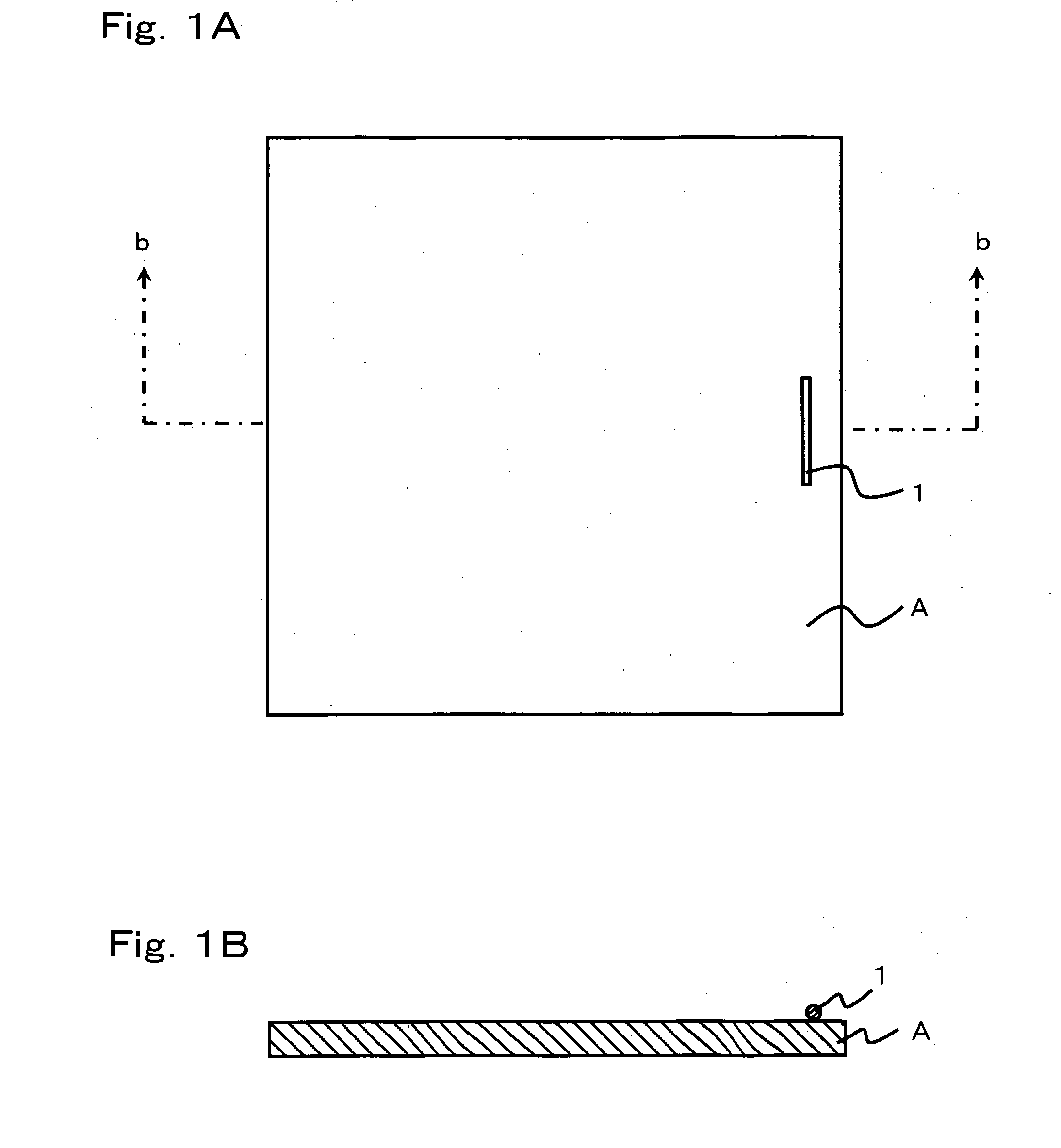
[0165] A glass substrate was set into an RF magnetron sputtering device (manufactured by Shimadzu Corp.), and the temperature of this glass substrate was set to 200° C. As illustrated in FIGS. 1, an Re metal wire 1 (diameter: 1 mmφ, a...

example 1-2

[0167] A transparent electroconductive film was produced in the same way as in Example 1-1 except that the Re wire was put onto a central position between the edge portion and the center of the sputtering target. In the transparent electroconductive film on the glass substrate, the value of [Re] / ([In]+[Zn]+[Re]), which represents the ratio of the atomic number of Re to the atomic number of all the metals, was 2.3×10⁻³. The resistivity, the carrier density, the mobility and the transmittance of this transparent electroconductive film were measured. As a result, they were 213 μ·Ω·cm, 9.72×10²⁰ / cm3, 30 cm2 / V·sec., and 89%, respectively (Table 1-1). The transparent electroconductive film was subjected to X-ray structural analysis. As a result, it was found out that the film was amorphous. In other words, the resultant transparent electroconductive film was an amorphous transparent electroconductive film having a low resistance.


PUM

PropertyMeasurementUnit
Temperatureaaaaaaaaaa
Diameteraaaaaaaaaa
Percent by volumeaaaaaaaaaa

Abstract

A transparent conductive film of low resistivity excelling in transparency and etching properties; a sputtering target as its raw material; an amorphous transparent electrode substrate having the transparent conductive film superimposed on a substrate; and a process for producing the same. In particular, an amorphous transparent conductive film comprising at least indium oxide and zinc oxide, which contains at least one third metal selected from among Re, Nb, W, Mo and Zr and satisfies the formulae: 0.75≦[In]/([In]+[Zn])≦0.95 (1) 1.0×10⁻⁴≦[M]/([In]+[Zn]+[M])≦1.0×10−2 (2) wherein [In][Zn] and [M] represent the atomicity of In, atomicity of Zn and atomicity of third metal, respectively. This amorphous transparent conductive film exhibits amorphism ensuring excellent etching processability and exhibits low specific resistance and high mobility.

Description

TECHNICAL FIELD [0001] The present invention relates to an amorphous transparent electroconductive film, and a sputtering target used in a production process thereof; and an amorphous transparent electrode substrate using the amorphous transparent electroconductive film, and a production process thereof. The invention relates in particular to an amorphous transparent electroconductive film used for a thin film transistor-liquid crystal display (TFT-LCD), a super twisted nematic-liquid crystal display (STN-LCD), a twisted nematic-liquid crystal display (TN-LCD), an organic electroluminescence (EL) and so on, and a sputtering target used in a production process thereof; and an amorphous transparent electrode substrate using this amorphous transparent electroconductive film, and a production process thereof. [0002] The present invention relates to a color filter for display. The invention relates in particular to a color filter for display characterized by the material of its electrode...

Claims


Application Information

Patent Timeline
IPC IPC(8): H01L21/00H01L31/00C23C14/08C23C14/34G02F1/1343G02F1/1362
CPCC23C14/086C23C14/3414G02F1/13439G02F2001/136222G02F1/136222G02F1/1335C23C14/08
Inventor INOUE, KAZUYOSHI
Owner IDEMITSU KOSAN CO LTD
Why Eureka
Try Eureka