Display device and manufacturing method thereof

a technology of a display device and a manufacturing method, which is applied in the field of semiconductor devices, can solve the problems of film crack generation in the level difference portion or part of the film that is not formed, and achieve the effects of preventing the short circuit of a light emitting element, low cost display, and shortening the manufacturing process

Active Publication Date: 2007-06-21
SEMICON ENERGY LAB CO LTD
View PDF46 Cites 95 Cited by
  • Summary
  • Abstract
  • Description
  • Claims
  • Application Information

AI Technical Summary

Benefits of technology

[0008] In view of the foregoing problem, it is an object of the present invention to shorten a manufacturing process by forming a pixel electrode and a film to be stacked over the pixel electrode using one resist mask.
[0010] According to this structure, disconnection of a pixel electrode in a level difference portion can be prevented. Disconnection refers that, by forming a film over a surface having a level difference portion, a crack is generated in the film in the level difference portion or part of the film is not formed owing to unfavorable coverage of the film in the level difference portion.
[0012] According to this structure, the metal film can be used as part of a light-shielding film, and alignment of the light-shielding film can be easily conducted.
[0014] According to this structure, short-circuit of a light emitting element can be prevented in an electroluminescent display device.
[0015] A pixel electrode and a metal film formed over part of the pixel electrode to be in contact therewith can be formed using one resist pattern. Two patterns of the pixel electrode and the metal film can be formed using one resist pattern; therefore, a manufacturing process can be shortened, and accordingly, a low-cost display device can be realized.
[0016] According to the present invention, the number of manufacturing steps can be decreased more than before, and a manufacturing cost of a semiconductor device can be lowered. In addition, disconnection of a pixel electrode in a level difference portion can be prevented because a metal film is formed over the pixel electrode to be in contact therewith. An inexpensive and highly reliable display device with less display failure can be formed.

Problems solved by technology

Disconnection refers that, by forming a film over a surface having a level difference portion, a crack is generated in the film in the level difference portion or part of the film is not formed owing to unfavorable coverage of the film in the level difference portion.

Method used


Image

  • Display device and manufacturing method thereof
  • Display device and manufacturing method thereof
  • Display device and manufacturing method thereof

Examples


embodiment mode 1

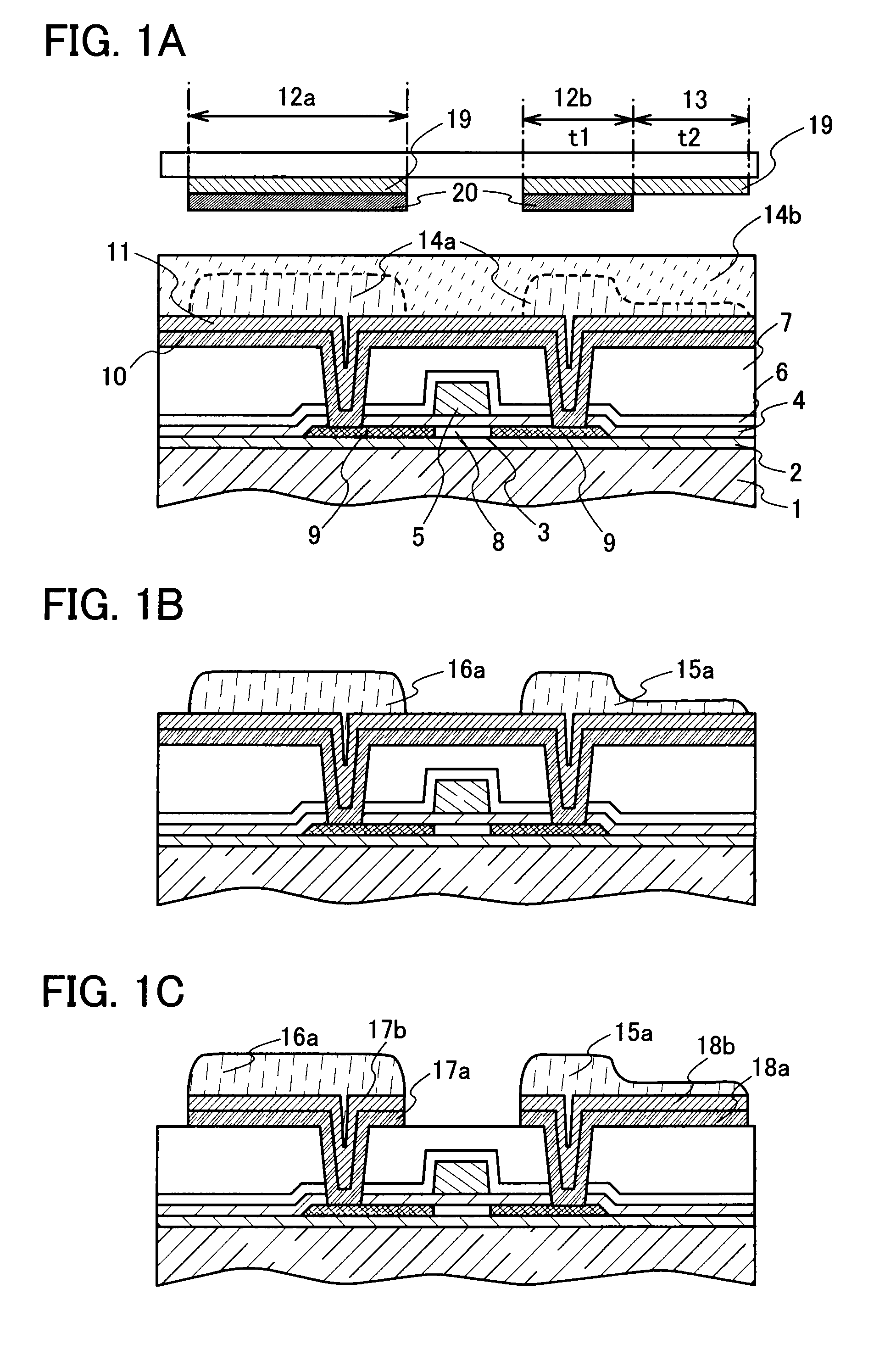
[0040] In this embodiment mode, a method for forming a top-gate TFT over a substrate 1 will be explained with reference to FIGS. 1A to 1C. The substrate 1 is a substrate having a light-transmitting property, for example, a quartz substrate, a glass substrate, or a plastic substrate. It is to be noted that the substrate 1 may be a substrate having a light-shielding property, and a semiconductor substrate or an SOI (Silicon on Insulator) substrate may be used.

[0041] An insulating film 2 is formed as a base film over the substrate 1. As the insulating film 2, a single layer of an insulating film such as a silicon oxide film, a silicon nitride film, or a silicon oxynitride film (SiOxNy), or a stack formed of at least two films of these films is used. Then, an island-like semiconductor film 3 is formed over the insulating film 2.

[0042] The island-like semiconductor film 3 is formed in the following manner: a semiconductor film is formed over the entire surface of the insulating film 2 ...

embodiment mode 2

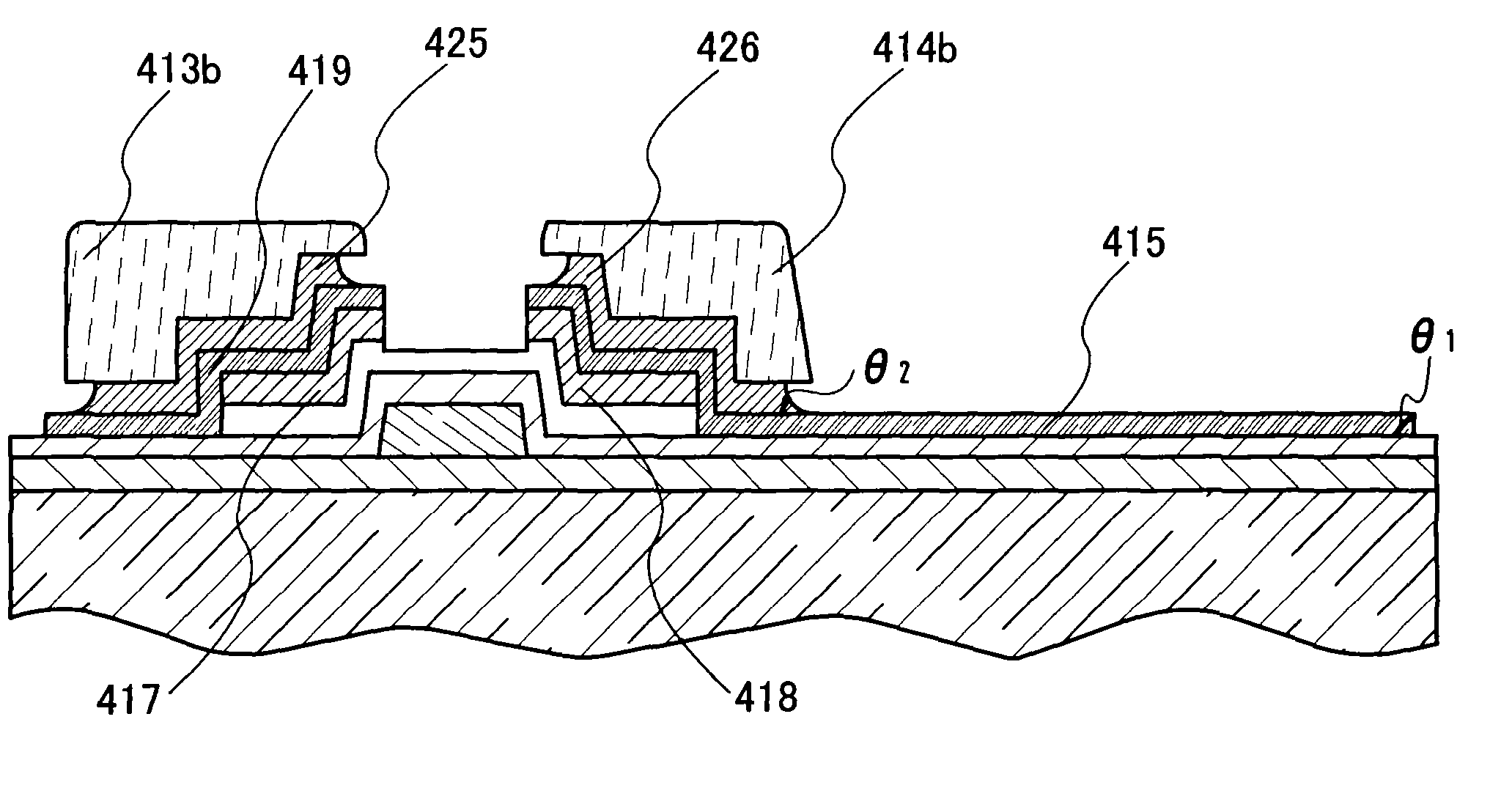
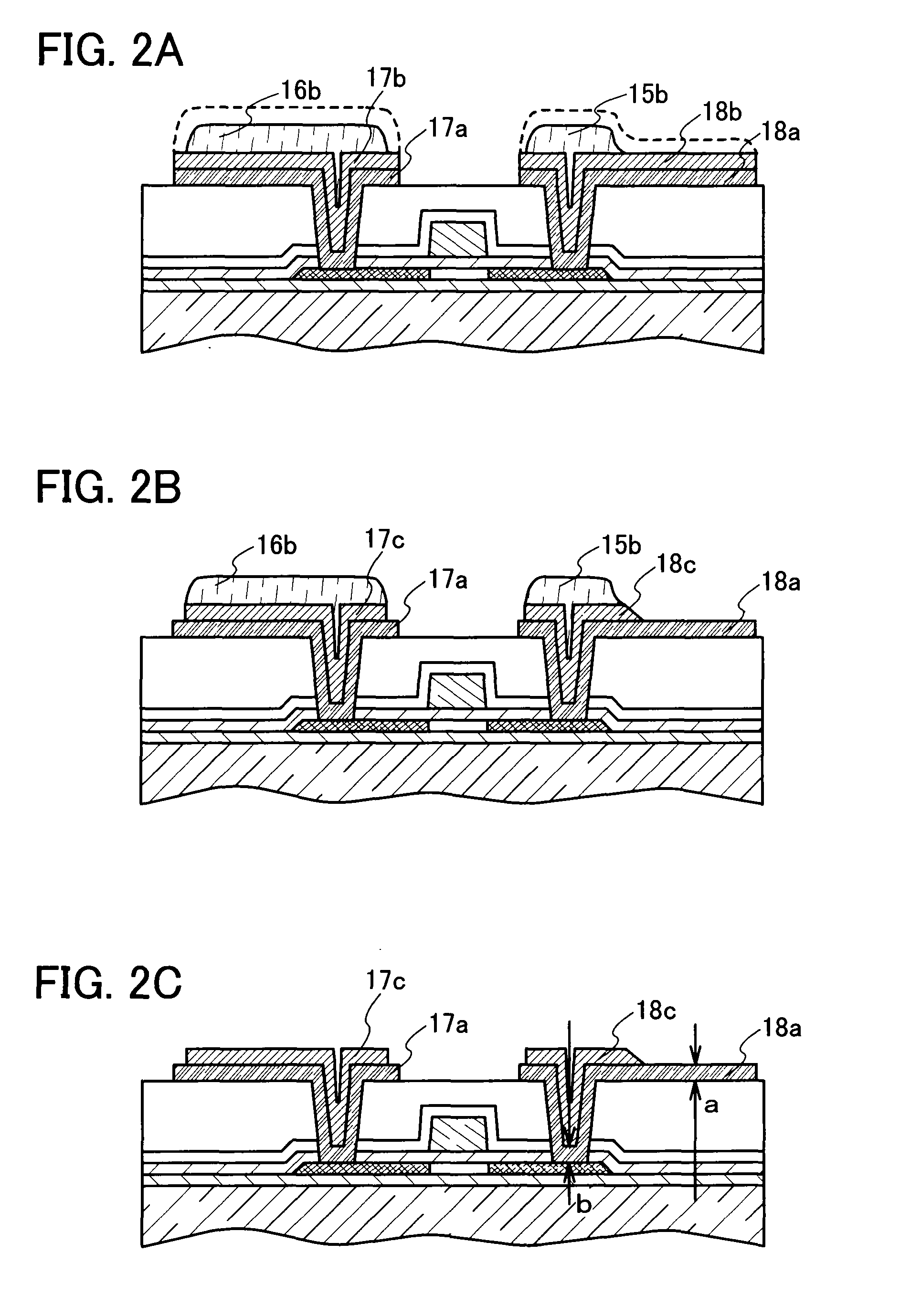
[0094] This embodiment mode will be explained with reference to FIGS. 5A to 5C. As for a forming method, a material, and the like of a type of a substrate and each layer which form a TFT to be explained in this embodiment mode, see Embodiment Mode 1.

[0095] An insulating film 402 is formed as a base film over a substrate 401. It is to be noted that a base film may not be provided. Then, a conductive layer is formed over the insulating film 402, and a shape of the conductive layer is processed using a mask formed by a photolithography method or the like to form a gate electrode 403.

[0096] A gate insulating film 404 is formed to cover the gate electrode 403. An amorphous semiconductor film is formed over the gate insulating film 404. Although there is no limitation on a material for the amorphous semiconductor film, the amorphous semiconductor film is favorably formed from silicon, a silicon-germanium (SiGe) alloy, or the like. Subsequently, a conductive layer is formed over the amor...

embodiment mode 3

[0128] In this embodiment mode, an exposure mask used in Embodiment Modes 1 and 2 will be explained with reference to FIGS. 11A to 11D. FIGS. 11A to 11C each show a top view of the light-shielding portion 12b and the semi light-transmitting portion 13 of the exposure mask shown in FIG. 1A or FIG. 5A. A width of the light-shielding portion 12b of the exposure mask is denoted by t1, and a width of the semi light-transmitting portion 13 thereof is denoted by t2.

[0129] The semi light-transmitting portion 13 can be provided with a diffraction grating pattern, and FIGS. 11A and 11B each show a diffraction grating pattern having a slit portion including a plurality of slits at or below a resolution limit of an exposure apparatus. The diffraction grating pattern is a pattern in which at least one pattern such as a slit or a dot is arranged. In a case where a plurality of patterns such as a slit or a dot is arranged, the patterns may be arranged periodically or aperiodically. By using a min...


PUM

PropertyMeasurementUnit
speedaaaaaaaaaa
lengthaaaaaaaaaa
thicknessaaaaaaaaaa

Abstract

It is an object of the present invention to form a pixel electrode and a metal film using one resist mask in manufacturing a stacked structure by forming the metal film over the pixel electrode. A conductive film to be a pixel electrode and a metal film are stacked. A resist pattern having a thick region and a region thinner than the thick region is formed over the metal film using an exposure mask having a semi light-transmitting portion. The pixel electrode, and the metal film formed over part of the pixel electrode to be in contact therewith are formed using the resist pattern. Accordingly, a pixel electrode and a metal film can be formed using one resist mask.

Description

BACKGROUND OF THE INVENTION [0001] 1. Field of the Invention [0002] The present invention relates to a semiconductor device having a pixel electrode, especially a display device. [0003] 2. Description of the Related Art [0004] In manufacturing an active matrix display device, in general, a wiring to be connected to a semiconductor film of a thin film transistor (TFT) is formed and a conductive film to be a pixel electrode is formed over the wiring. Therefore, a resist mask for forming the wiring and a resist mask for forming the pixel electrode have been required. [0005] Further, as another example, an example is given, in which a conductive film to be connected to a semiconductor film of a TFT is formed, the conductive film is made to serve also as a pixel electrode, and a metal film is formed over the conductive film (for example, Patent Document 1: Japanese Published Patent Application No. Hei 6-230425). This example is different from the example described above. A transparent co...

Claims


Application Information

Patent Timeline
Patent Type & Authority Applications(United States)
IPC IPC(8): G02F1/136G02F1/1343H05B44/00
CPCG02F1/133707G02F1/136209H01L29/458H01L51/5206H01L51/56H01L27/1214H01L27/1288H01L27/3276H01L27/3279H01L2227/323H01L27/124G02F1/133345H10K59/123H10K59/1315H10K59/131H10K50/814H10K59/1201H10K71/00H05B33/26H05B33/10G02F1/134336G02F1/136227G02F1/13629G02F1/134309G02F1/13439G02F2201/122G02F2201/123G02F1/136218H10K50/816H10K2102/103G02F1/133512G02F1/136286G02F1/1368
Inventor KIMURA, HAJIME
Owner SEMICON ENERGY LAB CO LTD
Why Eureka
Try Eureka