
Semiconductor device

a semiconductor device and wireless communication technology, applied in semiconductor devices, digital storage, instruments, etc., can solve the problems of increasing the current consumption of the semiconductor device as a whole, reading other unnecessary information, amplifying an enormous amount of current, etc., and achieves low power consumption and low cost. , the effect of low cos

Inactive Publication Date: 2007-06-28
SEMICON ENERGY LAB CO LTD
View PDF10 Cites 19 Cited by
  • Summary
  • Abstract
  • Description
  • Claims
  • Application Information

AI Technical Summary

Benefits of technology

[0007]As the nonvolatile storage device using a method of writing during manufacturing, there is a nonvolatile storage device called a mask ROM. In this nonvolatile storage device, a different photomask is used for every wireless chip. On the other hand, as the nonvolatile memory device using a method of writing after manufacturing, there is a nonvolatile storage device called an EPROM that is electrically writable. In other words, specific information is written in the EPROM using a writing device. In this case, different specific information is easily stored in the nonvolatile storage device for every wireless chip without changing a photomask.
[0008]In order to take out stored data from these nonvolatile storage devices, an address signal, a reading signal or the like is input to take out an electrical signal from a relevant storage element, and output information of a high potential signal or a low potential signal (hereinafter, the high potential signal is referred to as an “H” level, or simply “H,” and the low potential signal is referred to as an “L” level, or simply “L”) using a sense amplifier or the like. With such a nonvolatile storage device, a certain amount of time is required for reading necessary information, from the time reading is requested. Consequently, in order for a semiconductor device to be mounted with such a nonvolatile storage device, a design that takes this delay into consideration is necessary. Also, the sense amplifier consumes an enormous amount of current, which causes a rise in current consumption of the semiconductor device as a whole. Further, since the number of reading bits is set in such a nonvolatile storage device, even when only 1 bit is read, it is also necessary to read other unnecessary information. This further increases the current consumption in the semiconductor device.
[0009]In view of the foregoing problems, an object of the present invention is to reduce power consumption of a semiconductor device mounted with a nonvolatile storage device for storing specific information. Another object of the present invention is to reduce an affect of delay time from reading information from the nonvolatile storage device in the semiconductor device.
[0010]In a wireless chip according to the present invention, a nonvolatile storage circuit includes a storage element, which includes an electrical element including an electrically conducting or insulating means, a reset element, and a latch element. In the storage element, information is stored in the latch element by the reset element and the electrical element of the wireless chip when the wireless chip is reset. This information becomes “H” or “L” depending on whether the electrical element is electrically insulated or not. As the electrical element, an electrical resistor for which electrical insulation is possible by mechanical cutting by laser drawing, an electrical resistor and a diode for which electrical insulation is possible by thermal destruction by application of excess current, a phase change memory, a memory transistor including a floating gate, a memory transistor having a MONOS structure, or the like is possible.
[0011]By having a structure such as the foregoing, a wireless chip with low power consumption mounted with a nonvolatile storage device can be provided at low cost. Also, an increase in a circuit scale of the nonvolatile storage device can be suppressed because stored information can be read from the nonvolatile storage device without requiring a special circuit for reading such as a sense amplifier; therefore, a wireless chip mounted with a nonvolatile storage device with even smaller area and lower power consumption can be provided.
[0021]According to the present invention, a high performance and low power consumption wireless chip mounted with a nonvolatile storage device can be provided at low cost.

Problems solved by technology

Also, the sense amplifier consumes an enormous amount of current, which causes a rise in current consumption of the semiconductor device as a whole.
Further, since the number of reading bits is set in such a nonvolatile storage device, even when only 1 bit is read, it is also necessary to read other unnecessary information.
This further increases the current consumption in the semiconductor device.

Method used


Image

  • Semiconductor device
  • Semiconductor device
  • Semiconductor device

Examples


embodiment mode 1

(Embodiment Mode 1)

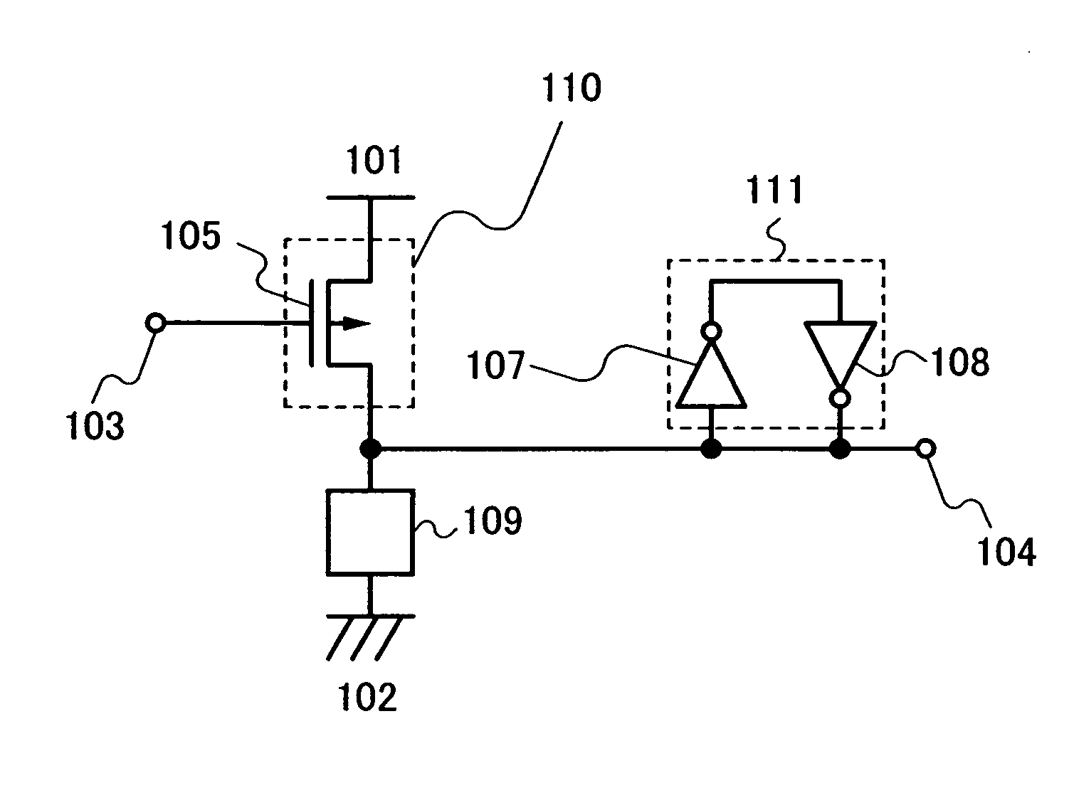
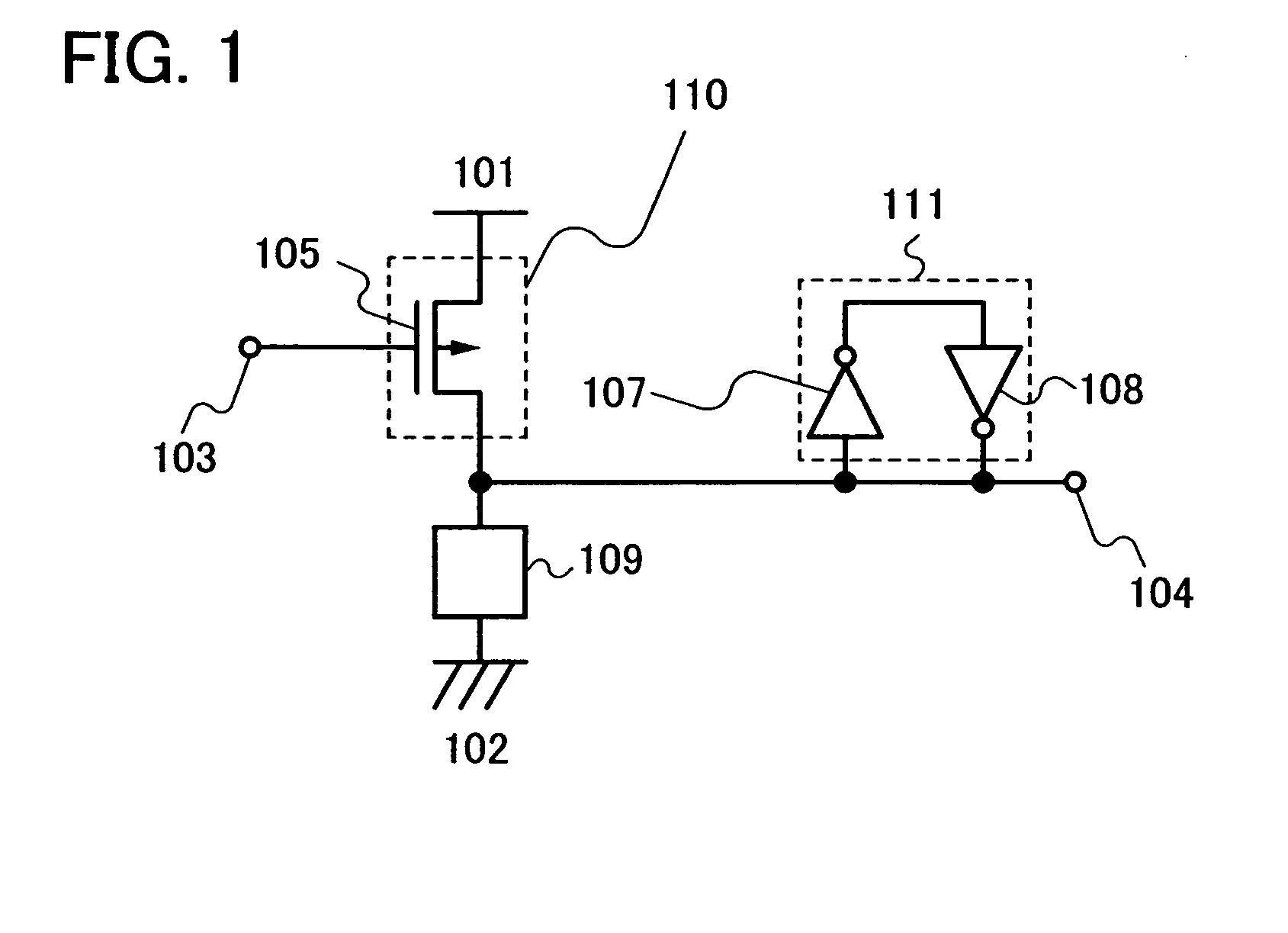
[0043]A first embodiment mode of a wireless chip according to the present invention is described with reference to FIG. 1. FIG. 1 shows a circuit diagram of a storage element of a nonvolatile storage device that is mounted to the wireless chip according to the present invention.

[0044]In FIG. 1, reference numerals 101, 102, 103, 104, 105, 107, 108, and 109 denote a power supply terminal, a ground terminal, a reset terminal, an output terminal, a P-type transistor, a first inverter, a second inverter, and an electronic element, respectively. The P-type transistor 105 forms the reset element 110. A source terminal, a drain terminal and a gate terminal of the P-type transistor 105 are connected to the power supply terminal 101, the output terminal 104, and the reset terminal 103, respectively. Also, the first inverter 107 and the second inverter 108 form a latch element 111.

[0045]As the electrical element, an electrical resistor for which electrical insulation is poss...

embodiment mode 2

(Embodiment Mode 2)

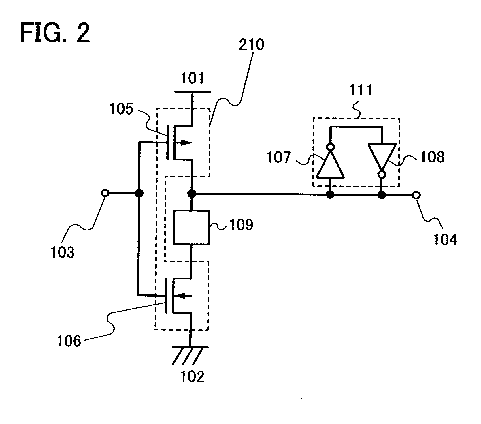
[0051]As a second embodiment mode of a wireless chip according to the present invention, a wireless chip with a structure different from that of the first embodiment mode is described with reference to FIG. 2. FIG. 2 is a circuit diagram of a storage element of a nonvolatile storage device that is mounted to the wireless chip according to the present invention.

[0052]FIG. 2 includes the power supply terminal 101, the ground terminal 102, the reset terminal 103, the output terminal 104, the P-type transistor 105, an N-type transistor 106, the first inverter 107, the second inverter 108, and the electrical element 109. The P-type transistor 105 and the N-type transistor 106 form a reset element 210. The source terminal, the drain terminal, and the gate terminal of the P-type transistor 105 are connected to the power supply terminal 101, the output terminal 104, and the reset terminal 103, respectively. A source terminal and a gate terminal of the N-type transistor 10...

embodiment 1

[0061]In this embodiment, an example of an electrical element that forms a nonvolatile storage device that is mounted to the wireless chip according to the present invention shown in Embodiment Mode 1 and Embodiment Mode 2 is described with reference to FIGS. 3A to 3C.

[0062]FIG. 3A is an example of forming an electrical element using an electrical resistor 301. A first terminal 302 and a second terminal 303 are electrically connected to the output terminal 104, and the ground terminal 102 of FIG. 1 described in Embodiment Mode 1, respectively. Also, the first terminal 302 and the second terminal 303 are electrically connected to the output terminal 104 and the N-type transistor 106 of FIG. 2 described in Embodiment Mode 2, respectively.

[0063]The electrical resistor 301 makes possible an electrical insulation by providing a region that is to be mechanically cut by laser drawing, and cutting this region by laser drawing. Also, the electrical resistor 301 makes possible an electrical i...


PUM


Abstract

Information stored in a nonvolatile storage device mounted to a semiconductor device is read by inputting an address signal or the like and by using a sense amplifier or the like. At this time, since a prescribed period of time is required, it is necessary to design a semiconductor device taking that delay into consideration. Also, a sense amplifier consumes an enormous amount of current. Further, since the number of reading bits is set, it is also necessary to read other unnecessary information when only 1 bit is to be read. A nonvolatile storage circuit is formed by a memory element that is formed by an electrical element having an electrically conducting or insulating means, a reset element, and a latch element. In the storage element, different information is stored in the latch element depending on whether the electrical element is electrically insulated or conductive, when the wireless chip is reset. With such a structure, a low power consumption wireless chip mounted with a nonvolatile storage device can be provided a low cost.

Description

BACKGROUND OF THE INVENTION[0001]1. Field of the Invention[0002]The present invention relates to a semiconductor device for wireless communication. In particular, the present invention relates to a semiconductor device in which a circuit formed using a semiconductor thin film transistor is supplied with a power supply voltage generated from a wireless communication signal.[0003]2. Description of the Related Art[0004]In recent years, a compact semiconductor device (hereinafter referred to as a wireless chip) that is a combination of an ultra compact IC chip and an antenna for wireless communication has received a lot of attention. Data can be written in and read from the wireless chip by transferring a communication signal using a wireless communication device (hereinafter referred to as a reader / writer).[0005]As an application field of the wireless chip, merchandise management in the distribution industry is given as an example. At present, merchandise management utilizing barcodes ...

Claims


Application Information

Patent Timeline
Patent Type & Authority Applications(United States)
IPC IPC(8): G11C7/00
CPCG11C16/30H01L21/8221H01L21/84H01L27/105H01L27/11526H01L27/11546H01L27/11551H01L27/1156H01L27/12H10B41/49H10B41/70H10B41/40H10B41/20H01L29/78645
Inventor KUROKAWA, YOSHIYUKI
Owner SEMICON ENERGY LAB CO LTD
Learn More