Semiconductor Device

Inactive Publication Date: 2007-06-28
LONGITUDE LICENSING LTD
View PDF8 Cites 32 Cited by
  • Summary
  • Abstract
  • Description
  • Claims
  • Application Information

AI Technical Summary

Benefits of technology

[0014]A semiconductor device according to the present invention comprises a memory cell array represented by DRAM array, input/output lines having a hierarchical structure, a sub-amplifier, a main amplifier, and a timing controller. The sub-amplifier amplifies faint signals read to lower input/output lines via the sense amplifier in the memory array. The sub-amplifier comprises, for example, a plurality of current sources having different conductance to each other and the current sources are activated independently by a plurality of read enable signals. The main amplifier amplifies faint voltage signal read to the upper input/output line via the sub-amplifier. The timing controller detects the number of cycles of burst read operation and generates a column select signal and a plurality of read enable signals with a timing according to the number of cycles. In a cycle of burst read operation just after bank activation, the timing controller activates a column signal and a first read enable signal with a timing later than that of subsequent cycles. With the first read enable signal, a current source having large conductance is activated and driving ability of the sub-amplifier is set to be high, thereby shortening data transfer time of the input/output lines (high speed mode). Therefore, in the memory array, it is possible to expand a read operation margin to realize read operation with high sp

Problems solved by technology

The first problem lies in that it is predicted that time required for reading stored data increases due to an RC delay (here, R represents wiring resistance and C represents load capacitance). FIG. 2 shows a diagram showing an example of an operation timing diagram in a read operation of a DDR SDRAM.
However, in consideration of the RC delay according to chip area of a DDR SDRAM of Gigabit class, since a row select operation time increases as shown in FIG. 3, a word line enable timing may delay by a time TRD0

Method used


Image

  • Semiconductor Device
  • Semiconductor Device
  • Semiconductor Device

Examples


first embodiment

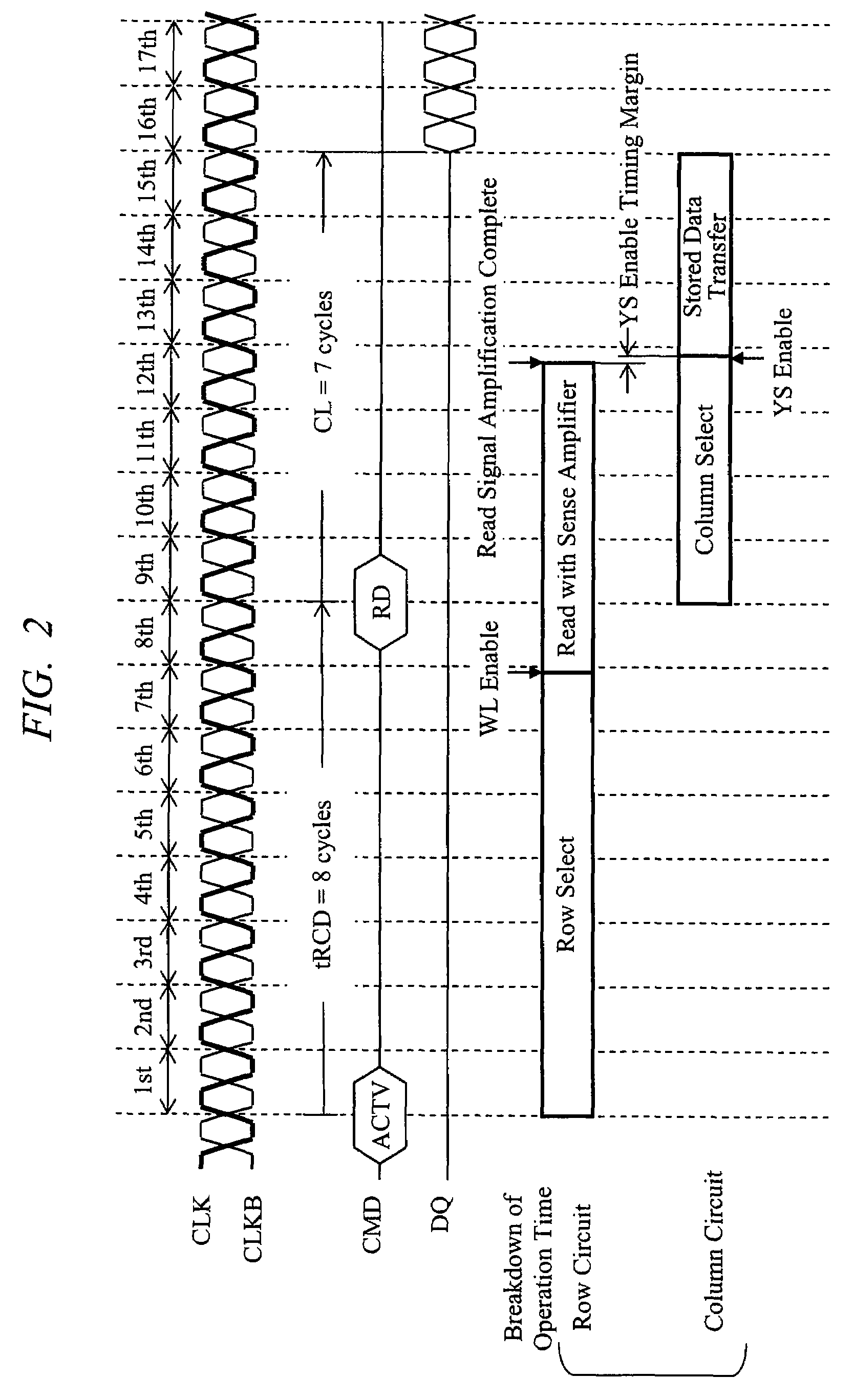
[0054]Features of the embodiment obtained from operation timing diagrams will be first described with reference to FIGS. 4 and 5. This embodiment has two major features. The first feature lies in that read circuit operation from a memory array to a main amplifier in a column circuit is speeded up. That is, circuit operation in the portion is shortened by overtime TD0 in a row circuit operation. FIG. 4 shows detailed breakdown of an optimal read operation time in the column circuit operation just after row circuit operation (so-called “page open”), in comparison with FIG. 3. TD1F represents a time required from enabling of a column select signal YS to activation of a main amplifier enable signal MAE, and the overtime TD0 is absorbed by shortening the time especially.

[0055]TD2 represents a time required from the activation of the main amplifier enable signal MAE to activation of a receiver amplifier enable signal RAE, TD3 represents a time required from the activation of a receiver am...

second embodiment

[0117]In a second embodiment, other configuration example and operation example of the current control circuit described in the first embodiment will be described.

[0118]FIG. 15 is a circuit diagram showing a configuration example of a column circuit different from that shown in FIG. 10 in a semiconductor device of the second embodiment according to the present invention. A feature of the configuration shown in FIG. 15 lies in that a current control circuit IC0A shown in FIG. 15 is composed of one NMOS transistor, which is different from the configuration shown in FIG. 10. The configuration shown in FIG. 15 is different from the configuration shown in FIG. 10 in the read enable signal is only RD12, it is connected to a gate electrode of the transistor N23, and voltage of the activated read enable signal RD12 varies according to respective burst read cycles.

[0119]FIG. 16 shows an operation timing diagram in read operation of the column circuit shown in FIG. 15. In the diagram, a read ...

third embodiment

[0123]In a third embodiment, another example of configuration and operation of the main amplifier used in the DDR SDRAM described in the first and second embodiment will be described. FIG. 19 is a circuit diagram showing a configuration example of a column circuit different from the column circuit shown in FIG. 10 and the like in a semiconductor device of the third embodiment according to the present invention. A feature of a main amplifier MAMP0A shown in FIG. 19 lies in that the main input / output line transmission gate MIOTG is removed from the circuit configuration shown in FIG. 10 and the cross-couple-type latch amplifier CCL2 is replaced with a gate input-type sense latch GIL.

[0124]The gate input-type sense latch GIL is composed of three PMOS transistors P51, P52, P53 and five NMOS transistors N51, N52, N53, N54, N55. The transistors P51, P52, N51, N52 form a positive feedback loop to amplify and hold current signals inputted from sources of the transistors N51, N52. Drains of ...


PUM


Abstract

A column circuit that amplifies signals read from a sense amplifier array SAA to local input/output lines LIO in sub-amplifiers SAMP to transfer the amplified signals to main input/output lines MIO is provided. A current control circuit IC that can set one of two kinds of currents according to read enable signals RD1, RD2 is provided in each sub-amplifier SAMP. The read enable signals RD1, RD2 are generated at timings corresponding to the number of cycles in burst read operation under control of the timing controller. Current in the current control circuit IC is set to be large by the RD1 in burst read operation cycle just after activation of a memory bank, while current in the current control circuit IC is set to be small by the RD2 in the next and subsequent burst read cycles. Accordingly, expansion of an operation margin or reduction of power consumption can be realized in a semiconductor device including a semiconductor memory such as a DRAM.

Description

CROSS-REFERENCE TO RELATED APPLICATION[0001]The present application claims priority from Japanese Patent Application No. JP 2005-378490 filed on Dec. 28, 2005, the content of which is hereby incorporated by reference into this application.TECHNICAL FIELD OF THE INVENTION[0002]The present invention relates to a semiconductor device, and particularly to a technique effectively applied to a semiconductor device having a semiconductor memory with a large storage capacity, and required for high-speed read operation.BACKGROUND OF THE INVENTION[0003]According to speed-up of a CPU, a demand for improvement of an operation frequency of a semiconductor memory is increasing year after year. In a conventional synchronous dynamic random access memory (SDRAM), speed-up has been achieved by raising an integration degree based upon miniaturization. In a double data rate synchronous dynamic random access memory (DDR SDRAM) which is currently mainstream, a data transfer rate has been improved by util...

Claims


Application Information

Patent Timeline
IPC IPC(8): G11C8/00
CPCG11C7/1012G11C7/1027G11C7/1048G11C7/1051G11C7/1066G11C7/1069G11C7/1072G11C7/1078G11C7/1096G11C7/12G11C7/22G11C11/4076G11C11/4091G11C11/4093G11C11/4094G11C11/4096G11C29/028G11C2207/002G11C11/40
Inventor HANZAWA, SATORUSEKIGUCHI, TOMONORITAKEMURA, RIICHIROAKIYAMA, SATORUKAJIGAYA, KAZUHIKO
Owner LONGITUDE LICENSING LTD
Why Eureka
Try Eureka