Two-dimensional photonic crystal
a photonic crystal and two-dimensional technology, applied in the field of two-dimensional photonic crystals, can solve the problems of document 1 not allowing the ff value to be equal or larger than 0.5, deteriorating the light propagation efficiency, etc., and achieve the effect of convenient manufacturing
- Summary
- Abstract
- Description
- Claims
- Application Information
AI Technical Summary
Benefits of technology
Problems solved by technology
Method used
Image
Examples
embodiments
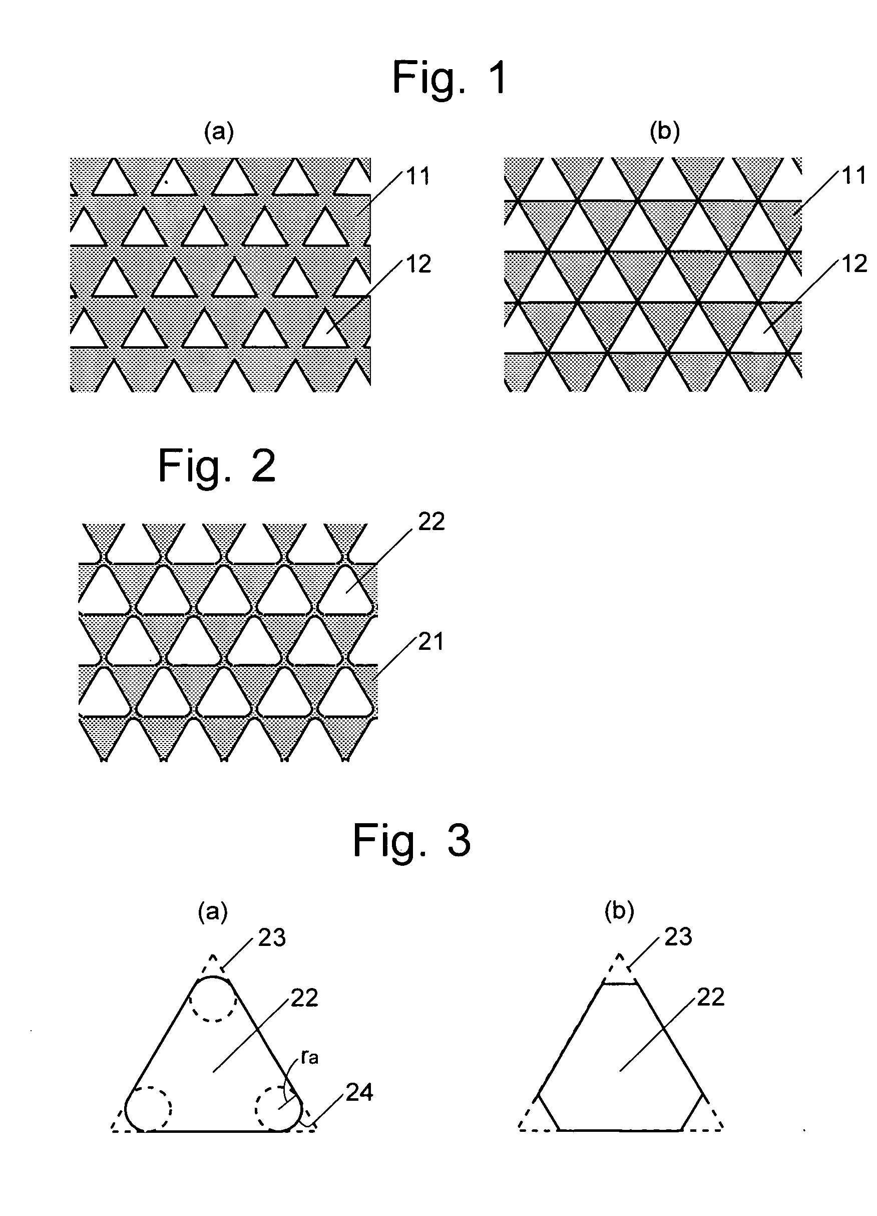
[0040] FIGS. 2 to 4 show an embodiment of the two-dimensional photonic crystal according to the present invention. As shown in FIG. 2, the two-dimensional photonic crystal of the present embodiment consists of a slab-shaped body 21 provided with holes 22 arranged in a triangular lattice pattern. As shown in FIG. 3(a), the basic shape of the holes 22 is an equilateral triangle 23 (broken line) whose corners are each removed along an arc 24 of an inscribed circle having a radius of ra.
[0041] Alternatively, it is possible to remove each corner along a straight line, as shown in FIG. 3(b). However, if an electron-beam drilling process is used to create the hole 22, the arc shape shown in (a) is desirable in that the electron beam leaves a circular edge that can be used as is.
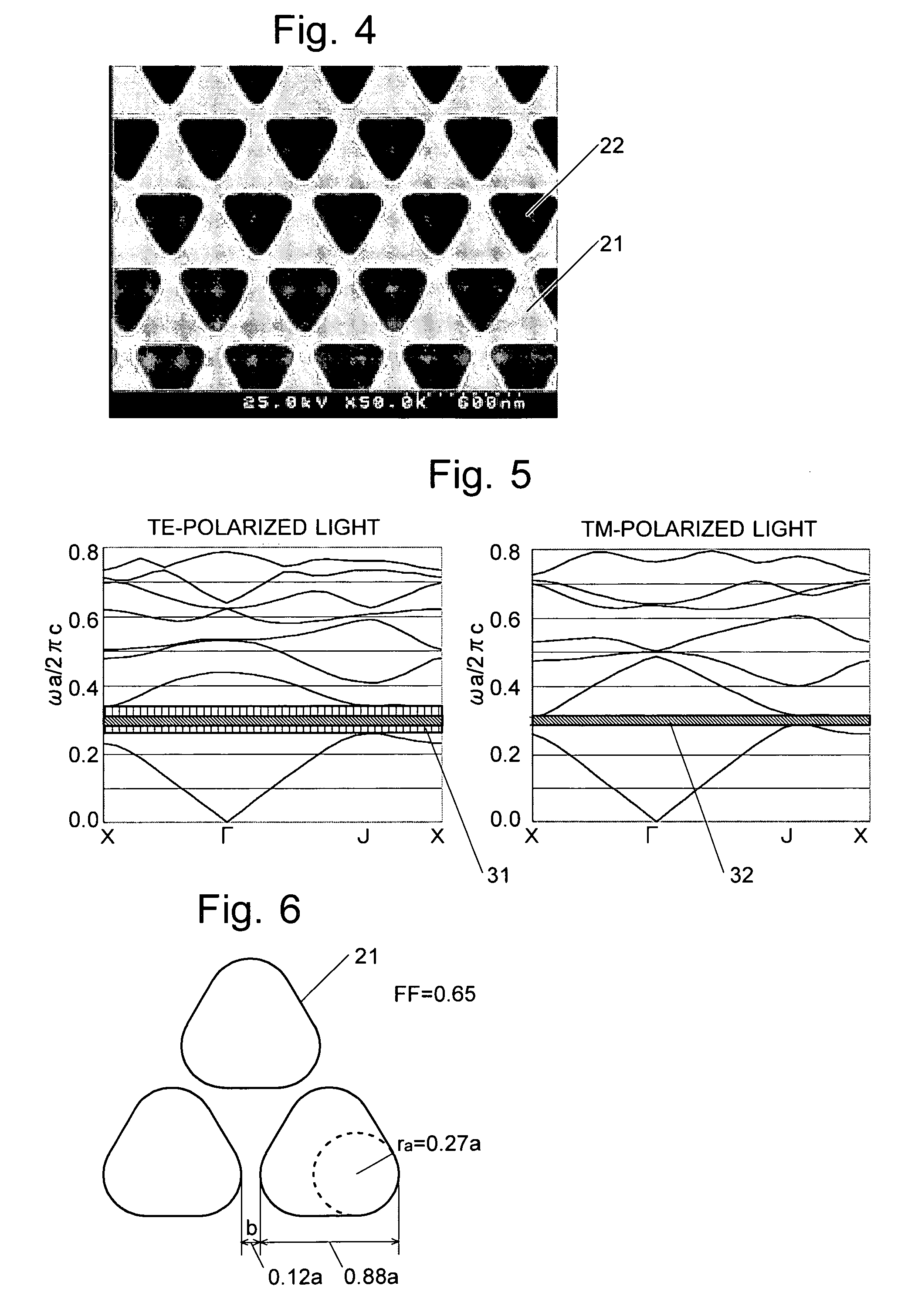
[0042]FIG. 4 shows an electron microscopic image of a two-dimensional photonic crystal actually manufactured, which consists of a slab-shaped silicon body 21 provided with neatly arranged holes 22 having an equila...
PUM
 Abstract
Description
Claims
Application Information


