Method for manufacturing a semiconductor device and laser irradiation method and laser irradiation apparatus

a laser irradiation and semiconductor technology, applied in the direction of semiconductor devices, electrical devices, basic electric elements, etc., can solve the problems of easy shape change, inferior heat resistance of glass substrates, etc., to reduce the region, reduce the proportion of long crystal grain regions, and reduce the size of the crystalline region.

Inactive Publication Date: 2007-08-09
SEMICON ENERGY LAB CO LTD
View PDF25 Cites 11 Cited by
  • Summary
  • Abstract
  • Description
  • Claims
  • Application Information

AI Technical Summary

Benefits of technology

[0090] When the laser annealing is performed by the constitution of the present invention, it becomes possible to make the inferior crystalline region as small as possible and to increase the proportion of the long crystal grain region formed on the semiconductor film. Therefore, it becomes possible to decrease the region in which TFT cannot be arranged and to integrate highly the semiconductor element. In the present invention, the fundamental wave having a wavelength of approximately 1 μm is irradiated supplementarily to the semiconductor film, which is the irradiated surface, simultaneously with the harmonic. Therefore, it is possible to suppress the sudden change in temperature of the semiconductor film and to assist the energy of the harmonic having small output effectively and so on. With these advantages satisfied, it is possible to enhance the operating characteristic and the reliability of the semiconductor device typified by an active matrix liquid crystal display device. Furthermore, it is possible to reduce the cost for manufacturing the semiconductor device. The present embodiment can be freely combined with any one of the embodiment modes 1 to 4 and the embodiment 1.

Problems solved by technology

The glass substrate, however, is inferior in heat resistance and easy to change in shape due to the heat.

Method used


Image

  • Method for manufacturing a semiconductor device and laser irradiation method and laser irradiation apparatus
  • Method for manufacturing a semiconductor device and laser irradiation method and laser irradiation apparatus
  • Method for manufacturing a semiconductor device and laser irradiation method and laser irradiation apparatus

Examples


embodiment mode 1

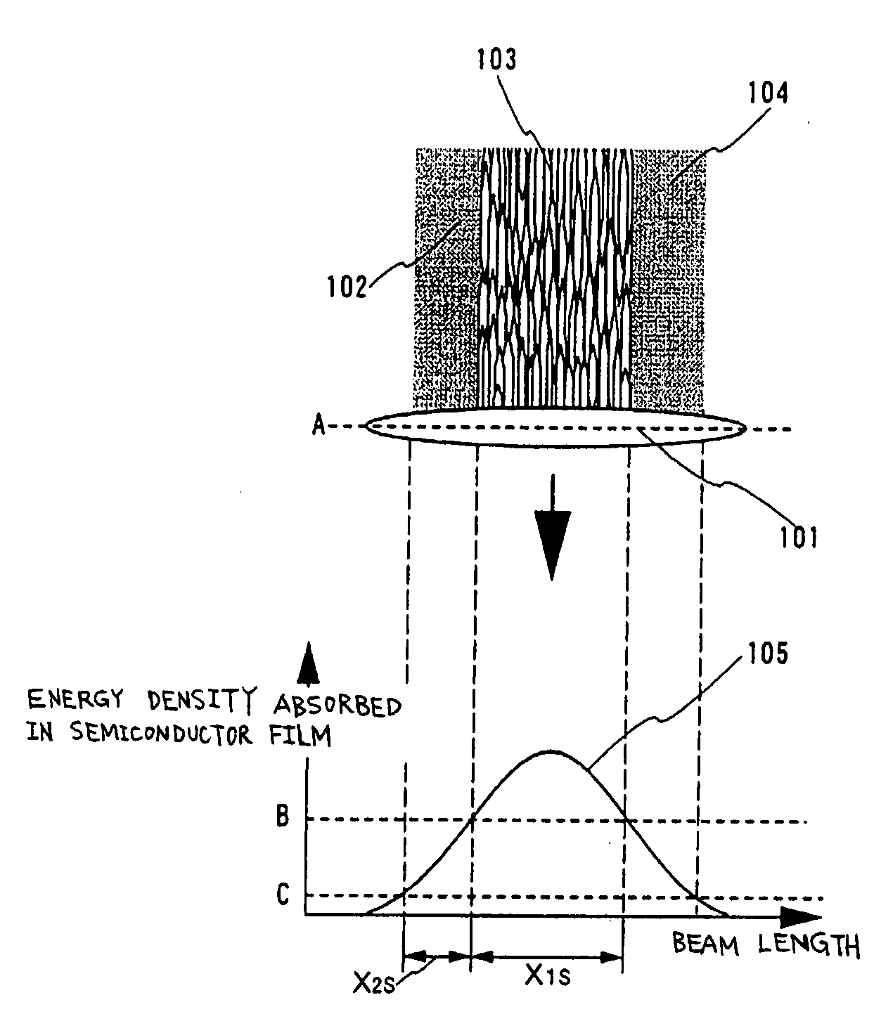
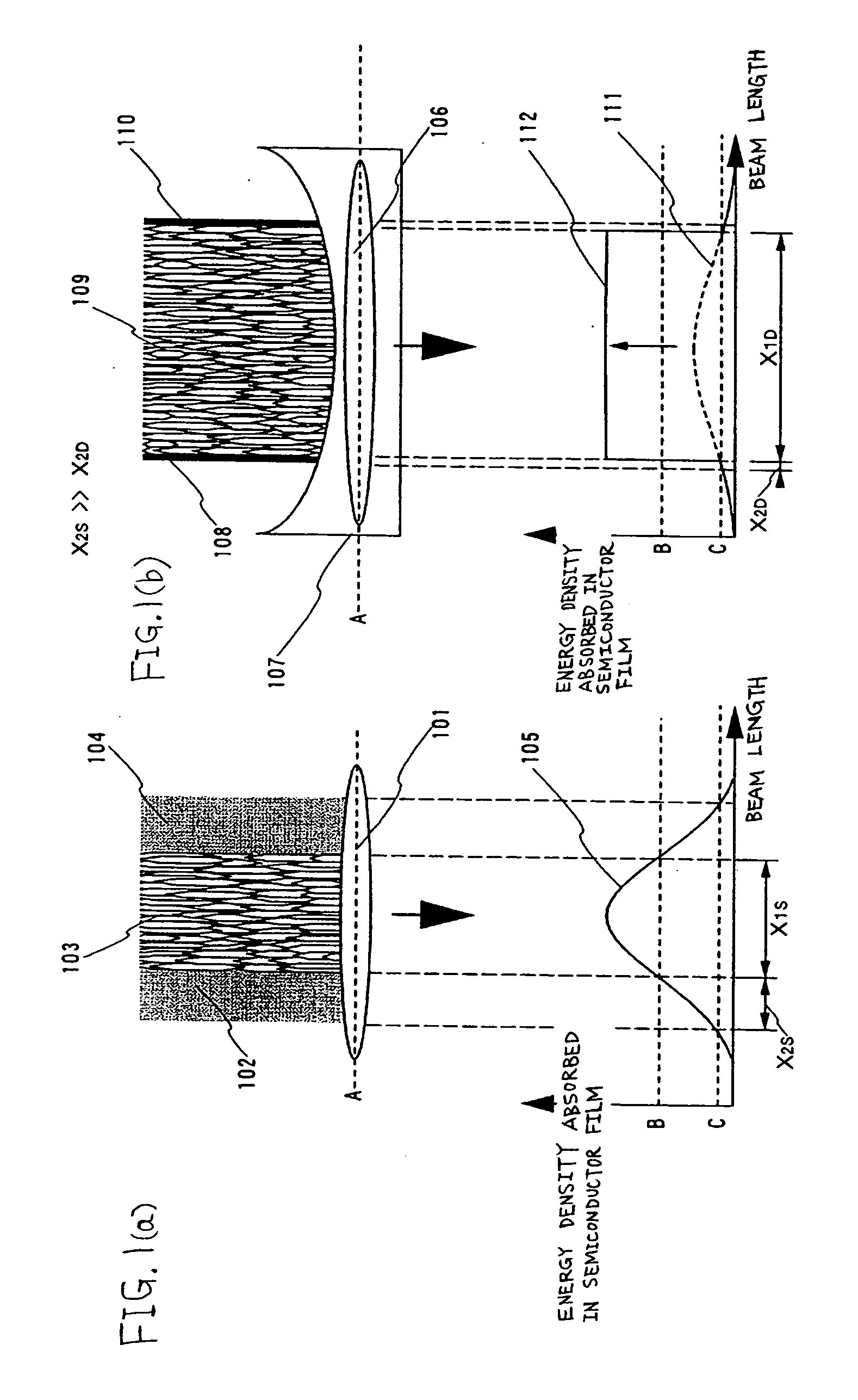
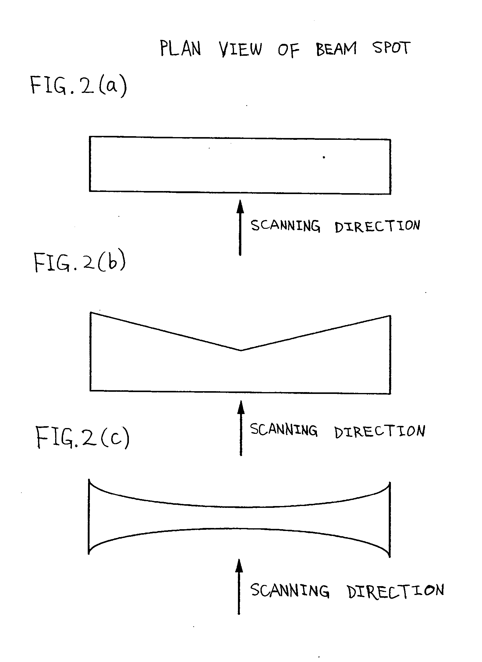
[0104] An embodiment mode of the present invention is explained with reference to FIG. 4. The present embodiment mode shows an example of forming a long beam 205 and a long beam 206 to irradiate a surface of a semiconductor film 204.

[0105] First, an LD pumped laser oscillator 201 (Nd:YVO4 laser, CW, the second harmonic (532 nm)) having an output of 10 W is prepared. The laser oscillator has an oscillation mode of TEM00 and has LBO crystal built in its resonator to convert into the second harmonic. Although it is not in particular necessary to limit to the second harmonic, the second harmonic is superior to the other higher harmonic in terms of energy efficiency. The beam has a diameter of 2.25 mm and a divergence angle of approximately 0.3 mrad. A 45° reflecting mirror 202 is used to change a traveling direction of the laser beam so as to have an angle of φ from the vertical direction. Next, the laser beam is made incident at an angle of φ into a planoconvex lens 203 having a focal...

embodiment mode 2

[0115] This embodiment mode explains an example in which several long beams obtained by shaping the second harmonics are combined to form a longer beam, and moreover, it is assisted with the energy of the fundamental wave with reference to FIG. 6.

[0116] First, four LD pumped laser oscillators each of which has an output of 10 W (Nd:YVO4 laser, CW, the second harmonic (532 nm)) are prepared (not shown in the figure). Each laser oscillator has an oscillation mode of TEM00 and the laser beam emitted from each laser oscillator is converted into the second harmonic through LBO crystal built in its resonator. The beam has a diameter of 2.25 mm and has a divergence angle of approximately 0.3 mrad. Several reflecting mirrors are used in order to change traveling directions of the respective laser beams so as to have an angle β to the vertical direction, and the laser beams are made incident into an irradiated surface from four directions so as to be combined into nearly one at the irradiat...

embodiment mode 3

[0122] This embodiment mode explains an example in which the long beam obtained by shaping the second harmonic is irradiated with the use of deflecting means such as a galvanometer mirror, and in addition, the laser beam of the fundamental wave is irradiated with the use of deflecting means such as a galvanometer mirror in order to assist the energy with reference to FIG. 7.

[0123] First, an LD pumped laser oscillator 601 having an output of 10 W (Nd:YVO4 laser, CW, the second harmonic (532 nm)) is prepared. The laser oscillator has an oscillation mode of TEM00 and the laser beam is converted into the second harmonic by LBO crystal built in its resonator. The beam has a diameter of 2.25 mm and has a divergence angle of approximately 0.3 mrad. Since this beam is circular, it is made incident into an optical system 602 for shaping it into oblong. A beam expander including two cylindrical lenses may be used as the shaping means for example, and the beam may be extended only in one dire...


PUM


Abstract

[Object]When the CW laser is employed for annealing the semiconductor film, a device having a high characteristic can be expected. On the other hand, when the beam shaped to be elliptical is scanned on the semiconductor film, a proportion of excimer-like crystal grain region becomes large and this is a problem in point of high integration. The present invention is to make the excimer-like crystal grain region formed over the semiconductor film as small as possible. [Solution]In the present invention, a fundamental wave having a wavelength of approximately 1 μm is irradiated supplementarily to the semiconductor film, which is the irradiated surface, simultaneously with a harmonic emitted from a CW laser. In addition, the fundamental wave is irradiated with a large amount of energy to a region irradiated by the harmonic with a small amount of energy, and the fundamental wave is irradiated with a small amount of energy to a region irradiated by the harmonic with a large amount of energy. Thus it becomes possible to form the long crystal grain region in the semiconductor film while suppressing the formation of the excimer-like crystal grain region.

Description

FIELD OF THE INVENTION [0001] The present invention relates to a laser irradiation method and to a laser irradiation apparatus (the apparatus includes a laser and an optical system to lead laser light output from the laser to an irradiated body) to perform the laser irradiation. In addition, the present invention also relates to a method for manufacturing a semiconductor device including a step of the laser processing. It is noted that the semiconductor device described herein indicates a general apparatus that can be functioned by utilizing a semiconductor characteristic including an electro-optical device such as a liquid crystal display device and a light-emitting apparatus, and an electronic device having the electro-optical device as its component. BACKGROUND ART [0002] In recent years, the technology to manufacture a thin film transistor (hereinafter referred to as TFT) over a substrate makes great progress and application development to an active matrix display device has bee...

Claims


Application Information

Patent Timeline
Patent Type & Authority Applications(United States)
IPC IPC(8): H01L21/84H01L21/00
CPCH01L21/2026H01L27/1296H01L27/1285H01L21/02683H01L21/02488H01L21/02422H01L21/02502H01L21/02496H01L21/0242H01L21/02425H01L21/02686H01L21/02678H01L21/02491H01L21/02532H01L21/02595H01L21/02381
Inventor TANAKA, KOICHIROOISHI, HIROTADAYAMAZAKI, SHUNPEI
Owner SEMICON ENERGY LAB CO LTD
Why Eureka
Try Eureka