Photodiode and method for fabricating same

a photodiode and photodiode technology, applied in the field of photodiodes, can solve the problems of reducing the utilization of signal light, reducing the sn ratio (signal-to-noise ratio), and increasing the vulnerability of the device to thermal noise, so as to achieve the effect of reducing the sn ratio

Inactive Publication Date: 2007-08-23
NEC CORP
View PDF9 Cites 93 Cited by
  • Summary
  • Abstract
  • Description
  • Claims
  • Application Information

AI Technical Summary

Benefits of technology

[0054] As should be clear from the foregoing explanation, the present invention can obtain a photodiode in which the junction electrical capacitance is extremely small, and through the use of this photodiode, a photoelectric conversion circuit having high-speed response can be produced. In addition, the ability to connect a greater load resistance in a series to the photodiode allows a signal output voltage to be obtained that is higher than that of the prior art. The ability to obtain a high signal output voltage in turn enables a reduction of the amplification rate of the amplifier that is provided in stages that follow the photoelectric conversion circuit or even allows the elimination of an amplifier altogether, which not only allows the configuration of the photoelectric conversion circuit to be simplified to reduce fabrication costs but also allows the realization of a photoelectric conversion circuit having low power consumption.

Problems solved by technology

However, when the load resistance is reduced to shorten the circuit time constant, the voltage level of the regeneration signal that can be extracted drops, the device becomes more susceptible to the effect of thermal noise and other noises, and the SN ratio (signal-to-noise ratio) is degraded.
However, decreasing the junction area reduces the utilization of the signal light, and this in turn gives rise to the problem of degradation of the SN ratio of the regeneration signal.
Although a lens can be used to condense and improve the utilization of the signal light, the provision of a lens not only increases the size of the photoelectric conversion device itself, but also entails the difficult operations of aligning the lens and photodiode and positioning the lens and optical fiber.
This type of MSM photodetector suffers from the problem that increasing the thickness of the semiconductor to raise the quantum efficiency causes an increase in the propagation distance of electrons and a consequent drop in the operation speed.
In this configuration, the width of the opening for generating near-field light determines the efficiency and the distance of drift of electrons in the depletion layer determines the response speed, but because the width of the phototransmissive insulation pattern is the width of the depletion layer as a Schottky photodiode, the width of the opening and the distance of drift of electrons cannot be independently set and high efficiency and high speed therefore cannot be simultaneously obtained in the photoreception device.
As a result, no investigation has been conducted into reducing the thickness of the depletion layer or reducing the size of the photoelectric conversion area to achieve an increase in the speed of photoelectric conversion.
As a result, a high SN ratio cannot be obtained in photoelectric conversion even when the optical transmission device disclosed in JP-A-2000-171763 is used to irradiate light that has been propagated from the aperture of the optical transmission device onto a photoreception device.
However, it is believed that when near-field light is introduced into a photodiode, the relatively low light absorption coefficient of the material that makes up the photodiode prevents irradiation of light to positions deep in the photodiode, whereby a sufficient photodetection current is not observed.

Method used


Image

  • Photodiode and method for fabricating same
  • Photodiode and method for fabricating same
  • Photodiode and method for fabricating same

Examples


first embodiment

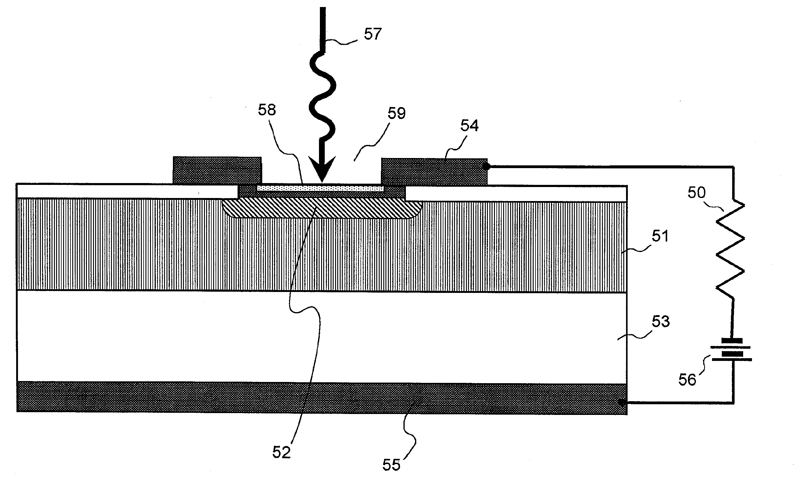
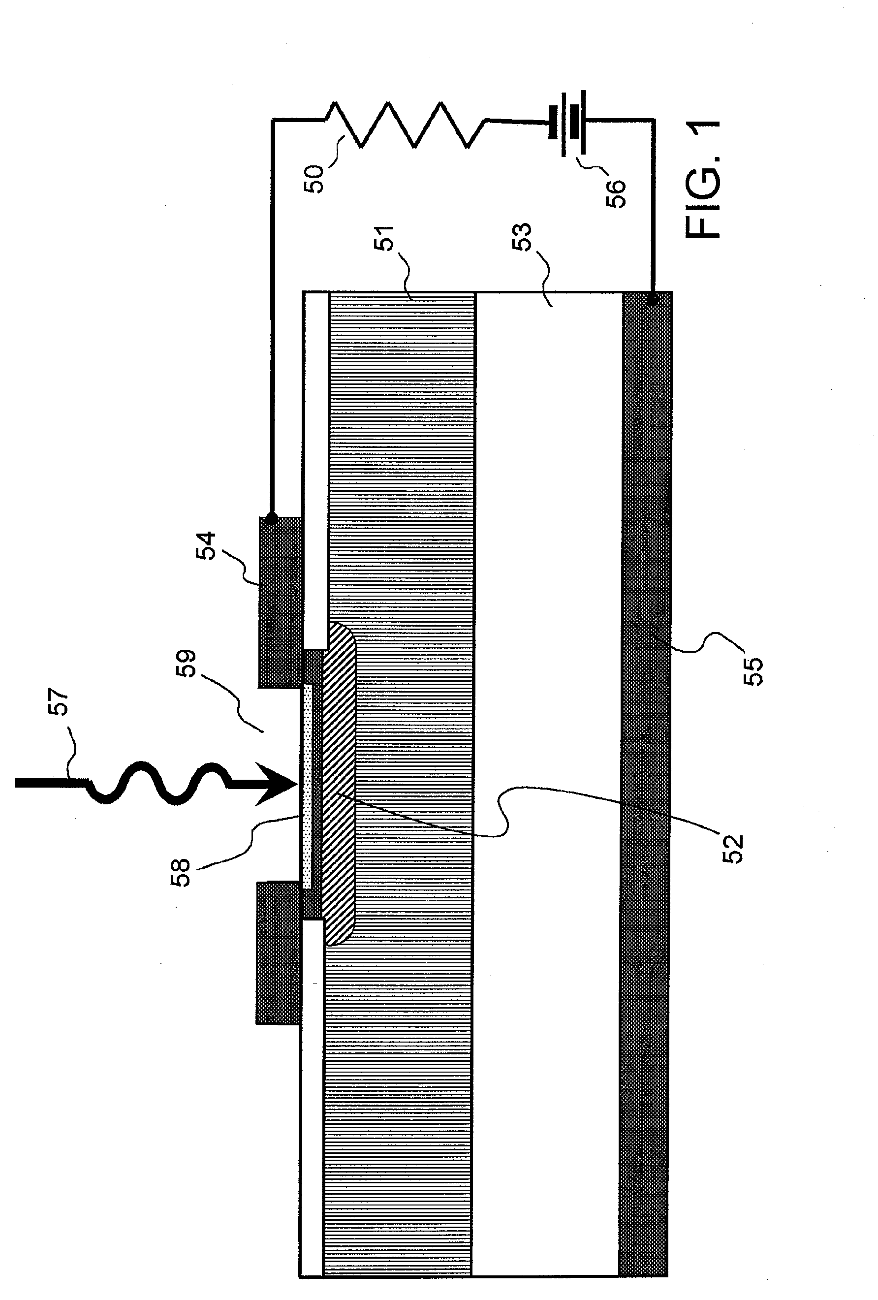
[0094] Explanation next regards a Schottky photodiode according to a first embodiment of the present invention. The Schottky photodiode of the first embodiment is configured as a planar photodiode. FIG. 4 is a partial sectional perspective view showing the overall configuration of this photodiode, and FIG. 5 shows an enlargement of this sectional view.

[0095] The Schottky photodiode shown in the figures is provided with: n+-type semiconductor layer 2 formed on a portion of substrate 1 such as SOI (Silicon-On-Insulator) in which the surface is insulating; n−-type semiconductor layer 3 provided on a portion of n+-type semiconductor layer 2; metal periodic structure member 4 that contacts n−-type semiconductor layer 3 and that has electrical conductivity; first electrode (anode electrode) 5 connected to metal periodic structure member 4; second electrode (cathode electrode) 8 that confronts first electrode 5 and contacts n+-type semiconductor layer 2; bias power supply 9 for applying a...
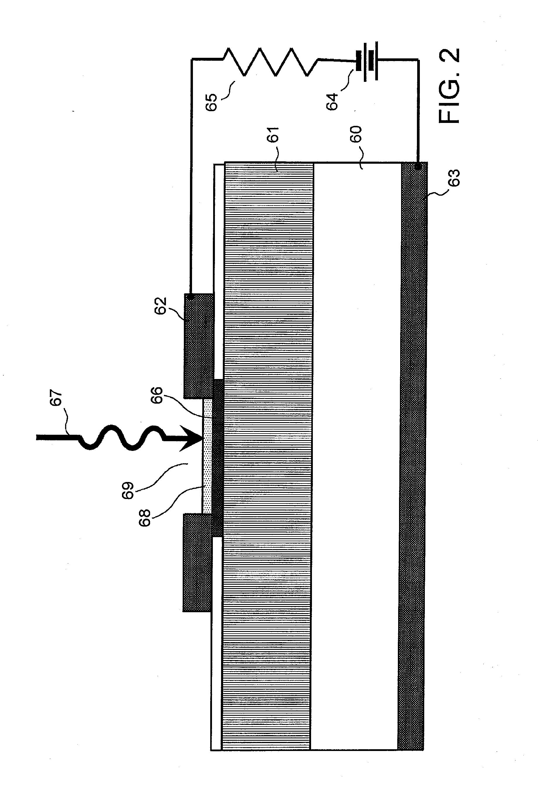
second embodiment

[0126] Explanation next regards the Schottky photodiode according to the second embodiment of the present invention. The photodiode of the first embodiment was of the planar type, but the photodiode of this second embodiment uses an insulating substrate and arranges the first electrode on the front surface of the substrate and the second electrode on the rear surface. FIG. 15 shows the configuration of a photodiode that is the second embodiment.

[0127] As in the case of the first embodiment, on the surface of insulating substrate 16, aperture 18 is provided at the center and metal periodic structure member 17 having a periodic structure realized by concentric surface irregularities is formed around aperture 18. As with the photodiode shown in FIGS. 4 to 6, aperture 18 does not completely penetrate metal periodic structure member 17. First electrode (anode electrode) 19 that is electrically connected to metal periodic structure member 17 is further provided on the surface of substrat...

third embodiment

[0132] Explanation next regards the Schottky photodiode according to the second embodiment of the present invention. The photodiode of the third embodiment shown in FIG. 16 is similar to the photodiode of the first embodiment but differs in that minute scattering member 40 for scattering light is provided on the bottom surface of aperture 6 provided in metal periodic structure member 4. As the material for this scattering member 40, a material in which the electrical resistance is low in the region of the wavelength of light is appropriate, and the same metal material as used for metal periodic structure member 4, for example, silver, gold or the like, can be used. The volume and shape of scattering member 40 has an influence on the state of surface plasmon resonance, scattering members 40 of sizes ranging from about 5 nm square to the same order as the wavelength of incident light exhibiting a broad range of effects. Scattering member 40 can have, for example, a cylindrical or squa...


PUM


Abstract

A Schottky photodiode includes a semiconductor layer and a conductive film provided in contact with the semiconductor layer. The conductive film has an aperture and a periodic structure provided around said aperture for producing a resonant state by an excited surface plasmon in a film surface of the conductive film by means of the incident light to the film surface. The photodiode detects near-field light that is generated by at the interface between the conductive film and semiconductor layer the excited surface plasmon. The aperture has a diameter smaller than the wavelength of the incident light.

Description

TECHNICAL FIELD [0001] The present invention relates to a photodiode for converting light signals that include invisible light such as infrared light to electrical signals at high speed, and to a method for fabricating the same. BACKGROUND ART [0002] Photodiodes are frequently used as devices for converting optical signals to electrical signals at high speed. Photodiodes are indispensable in the fields of information processing and communication. [0003] Various types of photodiodes are known, but a representative example of a photodiode for operating at high speed is the pin-type photodiode. As shown in FIG. 1, a pin-type photodiode is constituted from a semiconductor such as silicon and is of a configuration in which i-layer (intrinsic semiconductor layer) 51 is interposed between p-layer (p-type semiconductor layer) 52 and n-layer (n-type semiconductor layer) 53. P-layer 52 is formed as a thin layer on a portion of the surface of i-layer 51, and first electrode (anode electrode) 5...

Claims


Application Information

Patent Timeline
Patent Type & Authority Applications(United States)
IPC IPC(8): H01L31/113H01L31/0216H01L31/0224H01L31/108
CPCH01L31/108H01L31/022408H01L31/0216H01L31/10
Inventor OOHASHI, KEISHIISHI, TSUTOMUBABA, TOSHIOFUJIKATA, JUNICHIMAKITA, KIKUO
Owner NEC CORP
Why Eureka
Try Eureka