Defect inspection method and system

a technology of defect inspection and detection method, applied in the direction of material analysis, instruments, solid-state devices, etc., can solve the problems of low detective sensitivity, low detective sensitivity, and inability to readily achieve the effect of detecting and improving the sensitivity of detecting defects

Inactive Publication Date: 2007-09-06
HITACHI HIGH-TECH CORP
View PDF10 Cites 51 Cited by
  • Summary
  • Abstract
  • Description
  • Claims
  • Application Information

AI Technical Summary

Benefits of technology

[0010]The present invention addresses the foregoing problems. An object of the present invention is to provide a defect inspection method and system capable of inspecting an object of inspection on which repetitive patterns and non-repetitive patterns coexist so as to detect a microscopic foreign matter or defect quickly and highly precisely. In particular, the present invention provides a defect inspection method and system capable of stably detecting a microscopic foreign matter or defect while minimizing a difference in sensitivity between inspective areas, that is, a memory unit that includes many repetitive patterns and a logic unit in which non-repetitive patterns exist.
[0011]Moreover, another object of the present invention is to provide a defect inspection method and system that are attempted to improve the sensitivity in detecting a defect in a memory unit including many repetitive patterns. Herein, when a setting is designated for intercepting light, which is diffracted by patterns formed on a substrate to be inspected, at a position of a Fourier transform in a detective optical system using a spatial filter, the setting may be designated by employing either light diffracted by actual patterns or design data representing patterns. The setting of the spatial filter is designated prior to inspection of each of a plurality of memory units included in the same die. When each of the memory units is inspected, the setting of the spatial filter is automatically designated in order to highly sensitively detect a microscopic foreign matter or defect in the memory unit.
[0016]In another aspect of the present invention, there is employed a pulsed laser, which emits light that falls within the ultraviolet region, as a low-angle illumination light source. Moreover, one pulse of laser light emitted from the pulsed laser light source is split into a plurality of pulses in order to decrease the peak value of the laser light. The resultant laser light is irradiated to a specimen, whereby the damage the specimen incurs is reduced.

Problems solved by technology

However, the foregoing Prior Arts 1 to 5 cannot readily, highly sensitively, and quickly detect a microscopic foreign matter or defect on a substance on which repetitive patterns or non-repetitive patterns coexist.
Namely, the Prior Arts 1 to 5 are disadvantageous in a point that detective sensitivity (a minimum dimension of a foreign matter to be detected) is low except that for the repetitive patterns such as those realizing memory cells or the like.
Moreover, the Prior Arts 1 to 5 are disadvantageous in a point that the detective sensitivity is low relative to a microscopic foreign matter or defect of about 0.1 μm in a diameter existing in a highly densely patterned area.
Moreover, the Prior Arts 1 to 5 are disadvantageous in a point that the detective sensitivity is low relative to a foreign matter or defect which causes a short circuit of wiring, or a foreign matter shaped like a thin film.
Moreover, the Prior Art 6 is disadvantageous in a point that the precision in measurement of a foreign matter or defect is low.
Moreover, the Prior Art 6 is disadvantageous in a point that the detective sensitivity is low relative to a foreign matter on the surface of a wafer coated with a transparent thin film.

Method used


Image

  • Defect inspection method and system
  • Defect inspection method and system
  • Defect inspection method and system

Examples


first embodiment

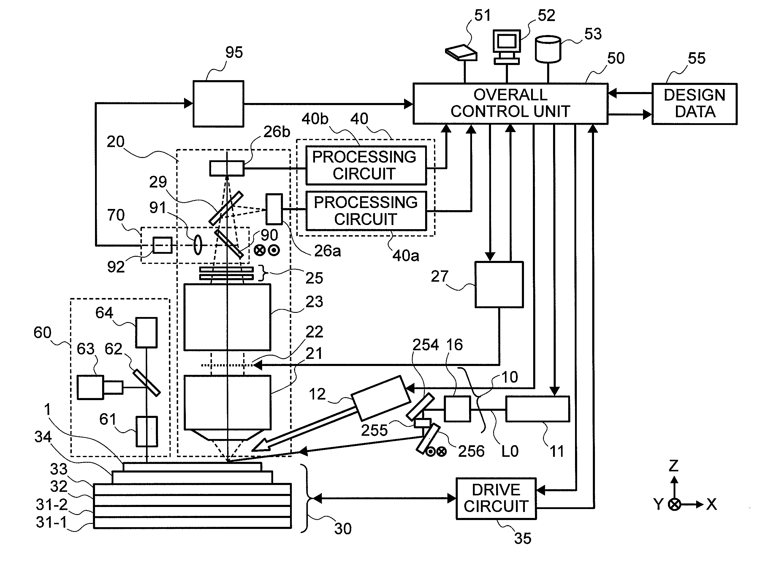
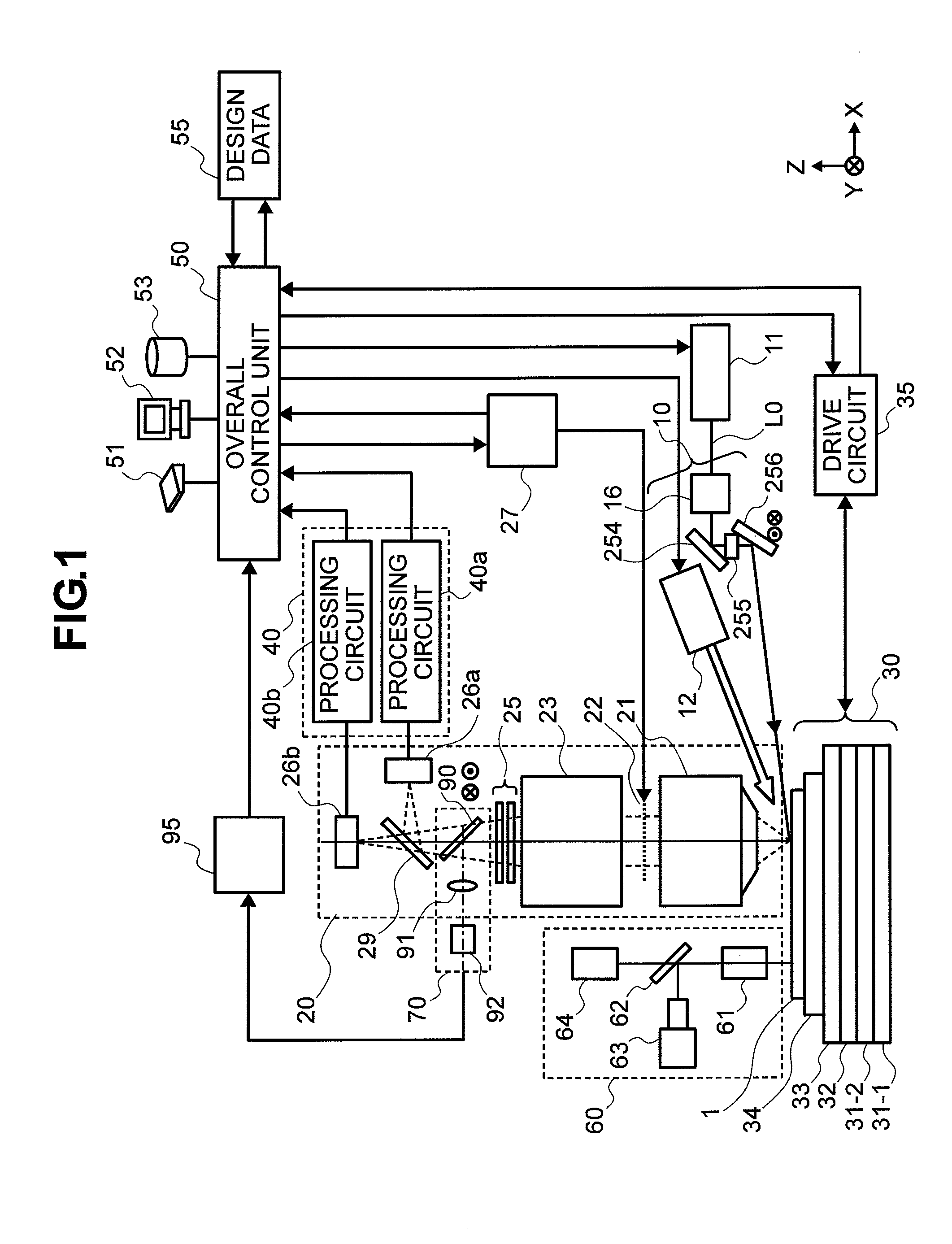
[0060]FIG. 1 shows the configuration of a defect inspection system in accordance with the first embodiment. The defect inspection system includes mainly an illuminative optical system 10, a variable-power detective optical system 20, a transportation system 30, a signal processing system 40, and an overall control unit 50 that controls the entire defect inspection system.

[0061]The transportation system 30 includes an X stage 31-1, a Y stage 21-2, a Z stage 32, and a θ stage 33 that are used to move a placement table bearing a substrate 1 to be inspected such as a wafer that is made of various materials through various manufacturing steps, and a drive circuit 35 that controls the stages.

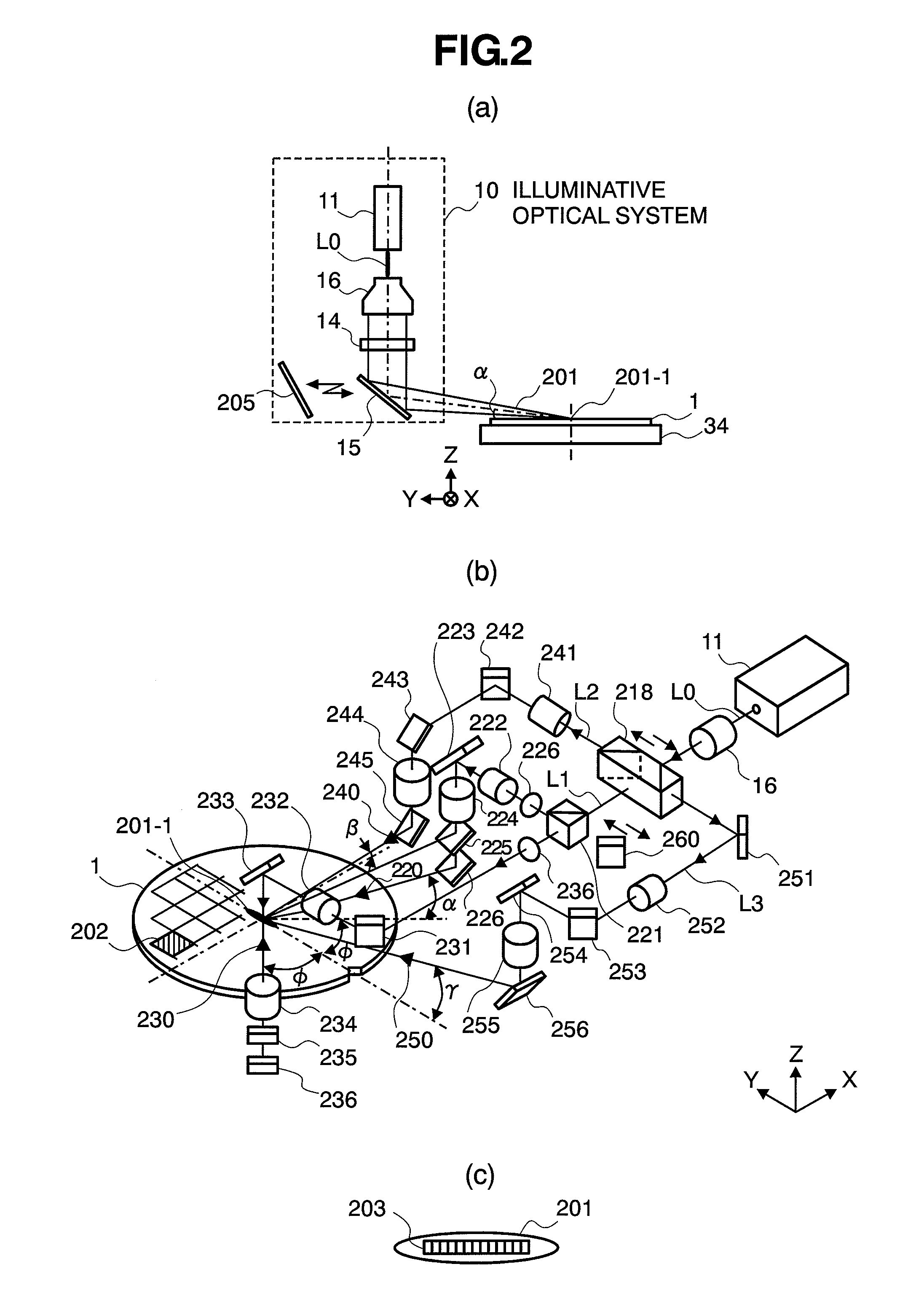
[0062]The illuminative optical system 10 includes an illumination light source 12 whose light falls in a wide wavelength band, a laser light source 11, a beam enlargement optical system 16, mirrors 254 and 256, and a lens 255. Light emitted from the laser light source 11 is enlarged to a certain size ...

second embodiment

[0147]During foreign matter inspection, even a multilayer wafer having a transparent film (for example, an oxide film) coated over the surface thereof must be inspected. The multilayer wafer is manufactured by repeating a step of forming patterns on the transparent film. There is an increasing need for detection of only foreign matters on the surface of an oxide film during inspection of a wafer having the oxide films formed therein. Fundamentally, by decreasing an illuminating angle α, an adverse effect of pattern-diffracted light or light reflected from a substrate can be suppressed. However, the decrease in the illuminating angle α poses a problem in that: light that is a regularly reflected component of illumination light, that is, forward scattered light occupies a majority of light scattered from a foreign matter; an amount of scattered light incident on a detective optical system located above gets smaller; and the foreign matter cannot therefore be detected stably.

[0148]In t...

third embodiment

[0156]FIG. 16 shows an embodiment of a defect inspection system including a microscope. In the present embodiment, a foreign matter detected during inspection can be verified using an observational optical system 60.

[0157]A detected foreign matter (including a quasi foreign matter) on the wafer 1 is moved to a position within a field of view offered by a microscope included in the observational optical system 60 by moving stages 31 and 32. The foreign matter is then observed.

[0158]The advantage provided by the inclusion of the observational optical system 60 lies in a point that a detected foreign matter can be immediately observed without the necessity of moving a wafer to a reviewer such as a scanning electron microscope (SEM). Since a foreign matter detected by an inspection system can be immediately observed, a cause of occurrence of the foreign matter can be identified quickly. Moreover, an image of a detected foreign matter picked up by a TV camera 64 included in the observati...


PUM

PropertyMeasurementUnit
tilt angleaaaaaaaaaa
angleaaaaaaaaaa
diameteraaaaaaaaaa

Abstract

An inspection system includes: a facility that uses wide-band illumination light having different wavelengths and single-wavelength light to perform dark-field illumination on an object of inspection, which has the surface thereof coated with a transparent film, in a plurality of illuminating directions at a plurality of illuminating angles; a facility that detects light reflected or scattered from repetitive patterns and light reflected or scattered from non-repetitive patterns with the wavelengths thereof separated from each other; a facility that efficiently detects light reflected or scattered from a foreign matter or defect in the repetitive patterns or non-repetitive patterns or a foreign matter or defect on the surface of the transparent film; and a facility that removes light, which is diffracted by the repetitive patterns, from a diffracted light image of actual patterns or design data representing patterns. Consequently, a more microscopic defect can be detected stably.

Description

BACKGROUND OF THE INVENTION[0001]1. Field of the Invention[0002]The present invention relates to a method and system for inspecting the occurrence of a foreign matter or defect in a device manufacturing process, wherein a foreign matter existent on a thin-film substrate, a semiconductor substrate, or a photomask, or a defect occurring in circuit patterns is detected in the course of manufacturing a semiconductor chip or a liquid crystal product, and the detected foreign matter or defect is analyzed in order to take measures.[0003]2. Description of the Related Art[0004]In a semiconductor manufacturing process, the presence of a foreign matter on a semiconductor substrate (wafer) causes a defective such as imperfect insulation of wiring or a short circuit thereof. Furthermore, due to the trend of semiconductor devices to a more and more microscopic structure, a more microscopic foreign mater brings about imperfect insulation of a capacitor or destruction of a gate oxide film. The fore...

Claims


Application Information

Patent Timeline
Patent Type & Authority Applications(United States)
IPC IPC(8): G01N21/88
CPCG01N21/21G01N21/4788G01N21/956G01N21/9501G01N21/94
Inventor UTO, SACHIONAKANO, HIROYUKISHIBATA, YUKIHIROHAMAMATSU, AKIRAURANO, YUTA
Owner HITACHI HIGH-TECH CORP
Why Eureka
Try Eureka