Manufacturing method for a circuit pattern, a thin film transistor and an electronic appliance

Inactive Publication Date: 2007-09-06
SEMICON ENERGY LAB CO LTD
View PDF30 Cites 40 Cited by
  • Summary
  • Abstract
  • Description
  • Claims
  • Application Information

AI Technical Summary

Benefits of technology

[0024]With a manufacturing method of the present invention, a desired pattern can be formed with good controllability. Therefore, a TFT with favorable electrical characteristics

Problems solved by technology

As described above, photolithography, which has been widely used in a conventional manufacturing process of a semiconductor, wastes large amount of materials and is difficult to be applied to a large substrate.
However, in an ink jet method, depending on a size of a discharge outlet of a nozzle from which a droplet is discharged, a scanning capability of the discharge outlet, and the like; it is difficult to precisely control discharge or the like of a pattern forming material.
Accordingly, sh

Method used


Image

  • Manufacturing method for a circuit pattern, a thin film transistor and an electronic appliance
  • Manufacturing method for a circuit pattern, a thin film transistor and an electronic appliance
  • Manufacturing method for a circuit pattern, a thin film transistor and an electronic appliance

Examples


embodiment mode 1

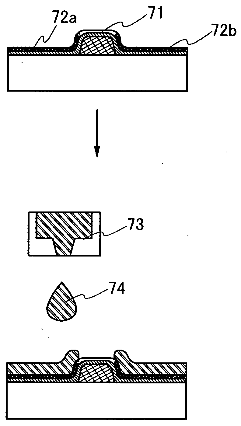
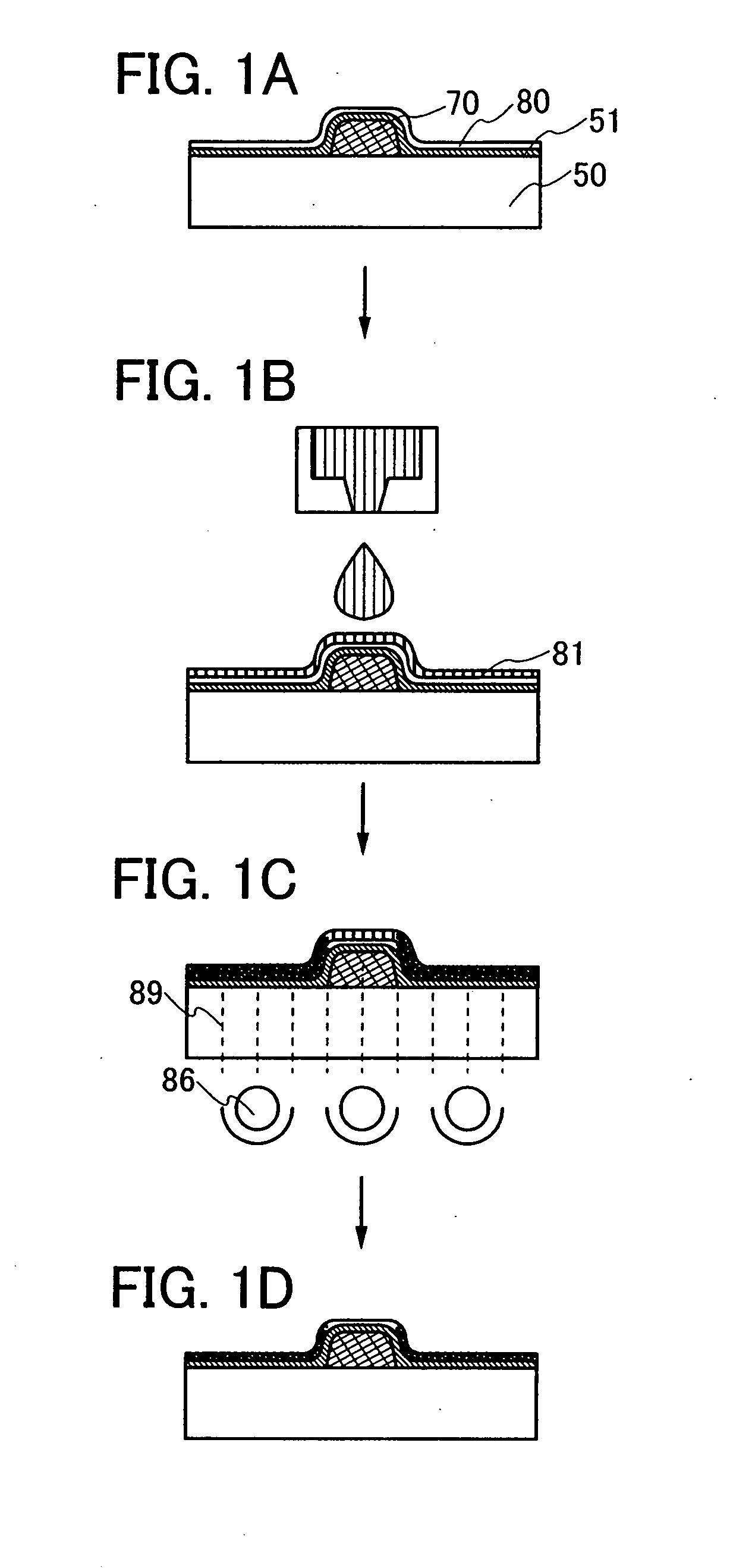
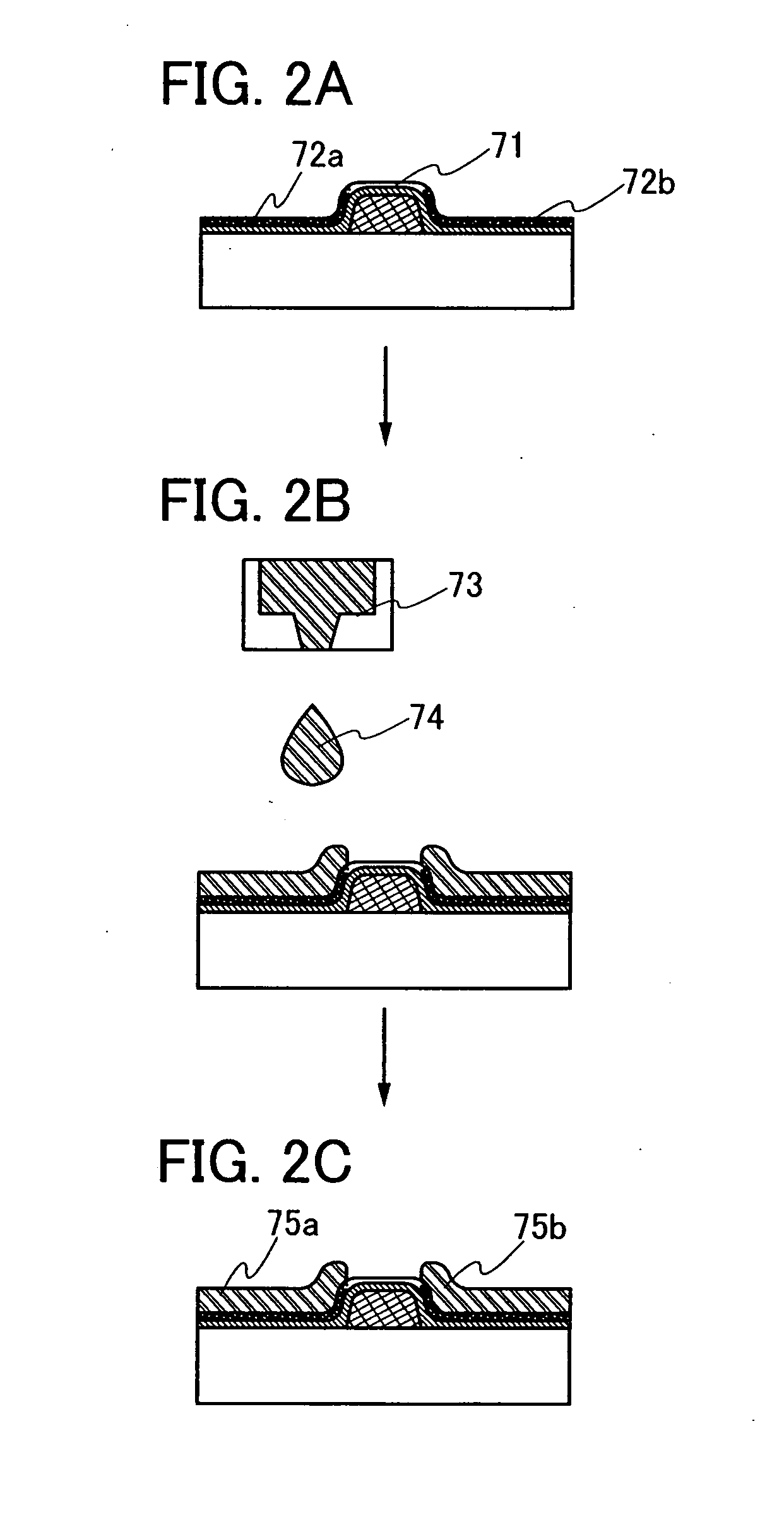
[0050]An example of an embodiment mode of the present invention is described with reference to FIGS. 1A to 2C.

[0051]In the present invention, a method in which one or more of patterns for forming a display device, such as a conductive layer for forming a wiring layer or an electrode, a mask layer for forming a predetermined pattern, and the like can be formed selectively is employed. In accordance with the present invention, a TFT, a display device including the TFT, a television device including the display device, and the like are manufactured. In the present invention, a pattern refers to any component elements in a TFT and a display device including the TFT, formed to have a predetermined shape such as a conductive layer such as a gate electrode layer, a source electrode layer, and a drain electrode layer; a semiconductor layer; a mask layer; an insulating layer; and the like. As a method for selectively forming a pattern, a droplet discharge (ejection) method (also referred to ...

embodiment mode 2

[0083]Hereinafter, a manufacturing method of a display device including a TFT manufactured by using the present invention is described with reference to FIGS. 3A to 13C and 15A to 17B. In each FIGS. 3 to 13, A is a top view of a pixel portion (a periphery of a TFT portion) in a display device and B and C are cross-sectional views along lines A-C and B-D in A, respectively.

[0084]As a light-transmitting substrate 100 in FIGS. 3A to 3C, a glass substrate, a quartz substrate, a silicon substrate, or the like is used. Alternatively, a plastic substrate with heat resistance capable of withstanding a processing temperature of the manufacturing step described later is used. Although not shown, an insulating layer may be formed over the light-transmitting substrate 100 as a base film. The insulating layer is formed by a CVD method, a plasma CVD method, a sputtering method, a spin coating method, or the like. The insulating layer may be a single layer or a stacked layer. Although formation of...

embodiment mode 3

[0152]In this embodiment mode, a light emitting device to which the present invention is applied is described. FIG. 21 shows an example of a light emitting device manufactured in accordance with the present invention. In FIG. 21, a pixel portion including a pixel is formed over a substrate 2800.

[0153]FIG. 21 shows a part of a section of a top emission light emitting display device including light emitting elements 2804 and 2805. Light is emitted in a direction shown by arrows in the drawing. Multicolor display can be carried out by setting different emission colors of red, green, and blue between neighboring pixels. In addition, by forming color layers 2807a, 2807b, and 2807c which correspond to light-emission colors at the sealing substrate 2820 side, color purity of light-emission colors can be improved. Alternatively, a pixel may include a white light emitting element and the color layers 2807a, 2807b, and 2807c may be combined.

[0154]The substrate 2800 is fixed to the sealing sub...


PUM

PropertyMeasurementUnit
Wavelengthaaaaaaaaaa
Photocatalytic propertiesaaaaaaaaaa
Electrical conductoraaaaaaaaaa

Abstract

A circuit pattern is formed by following steps: forming a light-blocking mask over a major surface of a light-transmitting substrate, forming a first film in a first region over the substrate and the mask, forming a photocatalytic film in at least a part of the first region over the first film, changing wettability of the first film in a second region which is in the first region, being in contact with the photocatalytic film, and not overlapping the mask, by light irradiation from a back surface opposite to the major surface of the substrate, removing the photocatalytic film, and forming a composition including a pattern forming material in the second region.

Description

BACKGROUND OF THE INVENTION[0001]1. Field of the Invention[0002]The present invention relates to a manufacturing method of a circuit pattern, a thin film transistor (hereinafter, also referred to as a TFT), and an electronic appliance using a droplet discharge method typified by an ink jet method and relates to a manufacturing method of a display device including the thin film transistor. In particular, the present invention relates to a manufacturing method of a circuit pattern such as a wiring, a thin film transistor, and an electronic appliance.[0003]2. Description of the Related Art[0004]In a manufacturing process of a thin film transistor and an electrical circuit including the thin film transistor, various kinds of thin films such as a semiconductor, an insulator, or a conductor are stacked over a substrate. In such a process, photolithography is widely known as a method for forming a pattern. A photolithography is a technique in which a pattern of a circuit or the like, which...

Claims


Application Information

Patent Timeline
IPC IPC(8): B05D5/12B05D1/32B29C71/04H01C17/06C23C30/00B41J3/407B05D5/00B05D3/00C23C24/00C23C18/00C08J7/18B29C71/02B29B15/10B28B19/00C04B41/00G02F1/1335H05K3/00C23C20/00C23C28/00C23C26/00
CPCC03C17/42C23C4/005C23C26/00C23C28/00H01C17/06H05K2203/1173H05K3/0082H05K3/1208H05K3/1241H05K2201/0108H05K2203/0551H01L51/0004C23C4/01H10K71/13
Inventor FUJII, GEN
Owner SEMICON ENERGY LAB CO LTD
Why Eureka
Try Eureka