Crystal preparing device, crystal preparing method, and crystal

a technology of crystal preparing device and crystal preparing method, which is applied in the direction of crystal growth process, crystal growth process, chemistry apparatus and processes, etc., can solve the problems of short operating life, deterioration of device characteristics, and inability to remove electrodes from such a substrate as in the conventional luminescence devi

Inactive Publication Date: 2007-09-20
RICOH KK
View PDF13 Cites 26 Cited by
  • Summary
  • Abstract
  • Description
  • Claims
  • Application Information

AI Technical Summary

Benefits of technology

[0017]According to one aspect of the invention, there is provided an improved cryst

Problems solved by technology

Such crystal defects relate directly to the drawbacks which cause deterioration of the device characteristics, for example, short operating life and heavy operation power in a luminescence device.
A sapphire substrate is an insulator, and taking out electrodes from such a substrate as in the conventional luminescence devices is impossible.
As a result, the area of the semiconductor device becomes large and there is a problem that the semiconductor device must be produced with high cost.
Moreover, if the area of the semiconductor device becomes large, another problem of a curvature of the substrate may arise due to the use of the combination of different materials: the substrate and the group III nitride semiconductor.
Moreover, in the case of the group III nitride semiconductor device produced on the sapphire substrate, performing the chip separation by cleavage is difficult and preparing the resonator end surface needed for a laser diode (LD) is difficult.
There

Method used


Image

  • Crystal preparing device, crystal preparing method, and crystal
  • Crystal preparing device, crystal preparing method, and crystal
  • Crystal preparing device, crystal preparing method, and crystal

Examples


Embodiment Construction

[0055]A description will be given of embodiments of the invention with reference to the accompanying drawings.

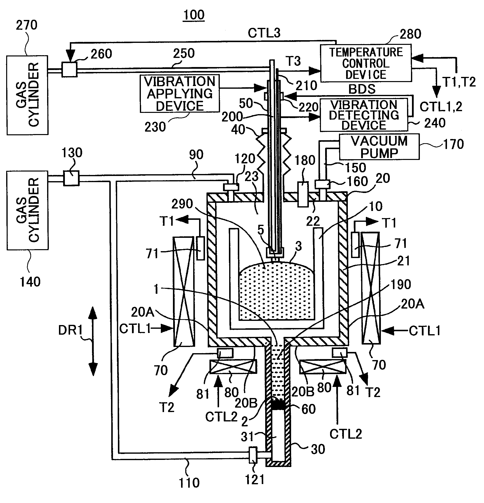
[0056]FIG. 1 shows the composition of a crystal preparing device in an embodiment of the invention. As shown in FIG. 1, the crystal preparing device 100 of this embodiment includes a crucible 10, a reaction container 20, piping 30, piping 200, a bellows 40, a supporting device 50, a molten metal holding member 60, heating devices 70, 80, temperature sensors 71, 81, gas supply lines 90, 110, 250, valves 120, 121, 160, a pressure regulator 130, gas cylinders 140, 270, an exhaust pipe 150, a vacuum pump 170, pressure sensor 180, molten metal 190, a thermocouple 210, an up-and-down movement device 220, a vibration applying device 230, a vibration detecting device 240, a flowmeter 260, and a temperature control device 280.

[0057]The crucible 10 has a generally cylindrical shape and is made of boron nitride (BN) or stainless steel (SUS316L). The reaction container 20 is arranged ar...


PUM


Abstract

In a crystal preparing device, a crucible holds a mixed molten metal containing alkali metal and group III metal. A container has a container space contacting the mixed molten metal and holds a molten alkali metal between the container space and an outside of the container, the molten alkali metal contacting the container space. A gas supply device supplies nitrogen gas to the container space. A heating device heats the crucible to a crystal growth temperature. The crystal preparing device is provided so that a vapor pressure of the alkali metal which evaporates from the molten alkali metal is substantially equal to a vapor pressure of the alkali metal which evaporates from the mixed molten metal.

Description

BACKGROUND OF THE INVENTION[0001]1. Field of the Invention[0002]The present invention relates to a crystal preparing device which carries out crystal growth of a group III nitride crystal, and a crystal preparing method which carries out crystal growth of a group III nitride crystal.[0003]2. Description of the Related Art[0004]Most of InGaAlN devices (or group III nitride semiconductor devices) which are currently used as ultraviolet, purple, blue, or green light sources are produced by carrying out crystal growth of a group III nitride crystal on a sapphire or silicone carbide (SiC) substrate by using the MOCVD method (organic metal chemical vapor deposition), the MBE method (molecular beam crystal growth method), etc.[0005]When sapphire and silicone carbide are used as the substrate in this case, the substrate and the group III nitride semiconductor greatly differ in the coefficient of thermal expansion and the grating constant, and many crystal defects will be included in the gro...

Claims


Application Information

Patent Timeline
IPC IPC(8): C30B9/00C01B21/06C30B11/00
CPCC30B9/10C30B17/00Y10T117/1024C30B29/406C30B29/403
Inventor IWATA, HIROKAZUSARAYAMA, SEIJIFUSE, AKIHIRO
Owner RICOH KK
Why Eureka
Try Eureka