Semiconductor device

a technology of switching element and semiconductor, applied in the direction of semiconductor devices, basic electric elements, electrical equipment, etc., can solve the problems of excessive energy of ion implantation and excessive time of impurity diffusion, and achieve the effect of low loss

Inactive Publication Date: 2007-09-27
HITACHI LTD
View PDF0 Cites 40 Cited by
  • Summary
  • Abstract
  • Description
  • Claims
  • Application Information

AI Technical Summary

Benefits of technology

[0012]In accordance with the present invention, a wide bandgap semiconductor switching element operable under the high withstanding...

Problems solved by technology

Among the above-described conventional technical ideas, although the patent publication 1 discloses such a structure that the wide band gap semiconductor is contacted to the silicon semiconductor, this patent publication 1 has not sufficiently considered the following points: That is, this contact plane is operated as a diode, and this junction is not operable under high withstanding voltage.
However, this patent publication 2 has not considered the manufacturing method and the semiconductor device structure, which ar...

Method used


Image

  • Semiconductor device
  • Semiconductor device
  • Semiconductor device

Examples


embodiment 1

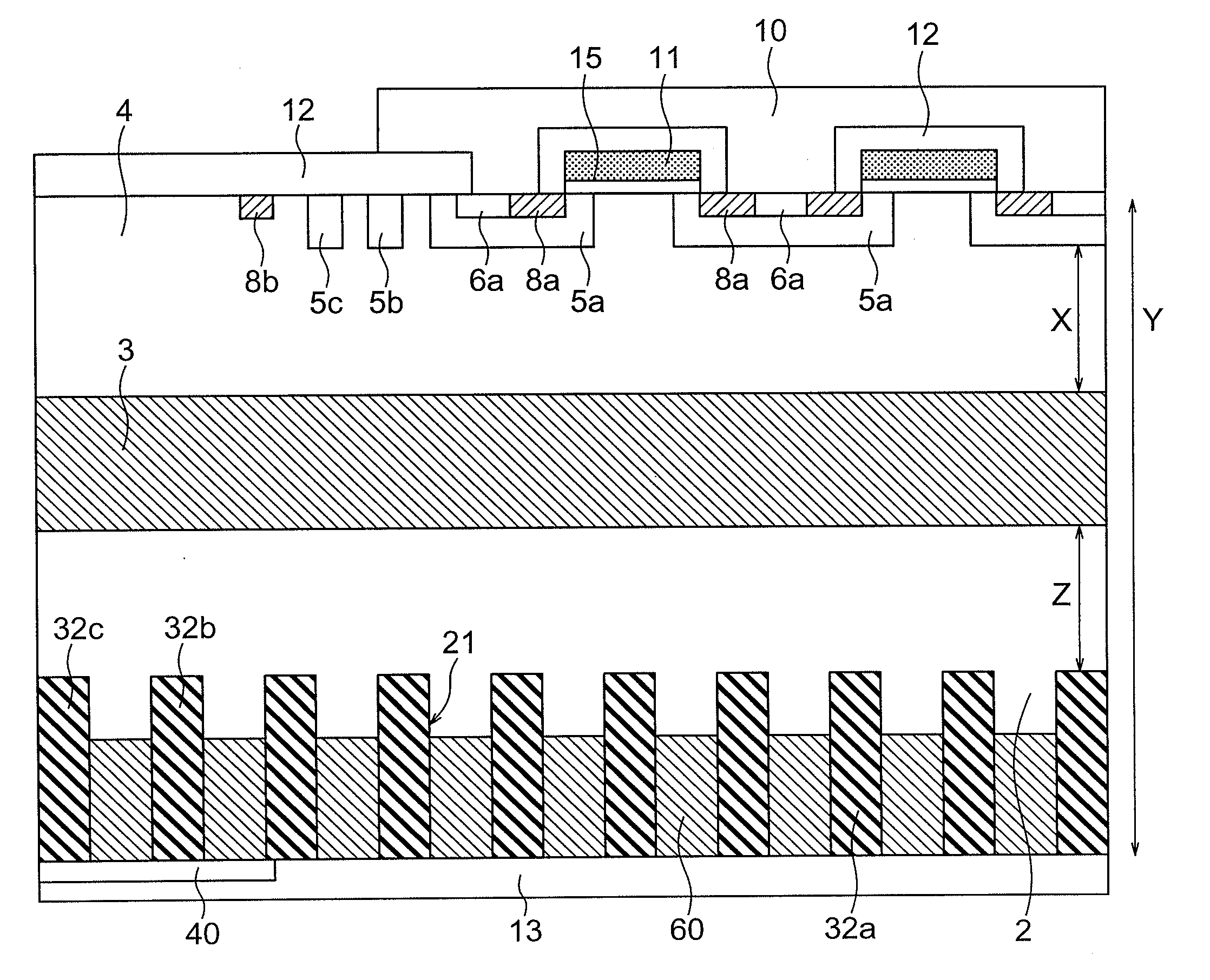
[0028]FIG. 1 is a semiconductor device of an embodiment 1 of the present invention. The semiconductor device of this embodiment 1 corresponds to a reverse blocking type SiC power MOSFET in which an SiC power MOSFET has been formed on the side of a first major plane, and a hetero junction diode has been formed between a polycrystal silicon semiconductor region 1 on the side of a second major plane and an n type SiC semiconductor region 4. In other words, an electrode layer 10 is a source electrode of the SiC power MOSFET, and the n type SiC semiconductor region 4 constitutes a drain region. However, the n type SiC semiconductor region 4 also constitutes a cathode region of the hetero junction diode, and the silicon semiconductor region 1 functions as an anode region of the hetero junction diode. As a consequence, an electrode layer 13 will be referred to as an anode electrode of the semiconductor device of this embodiment 1.

[0029]On the side of the first major plane, a p type body re...

embodiment 2

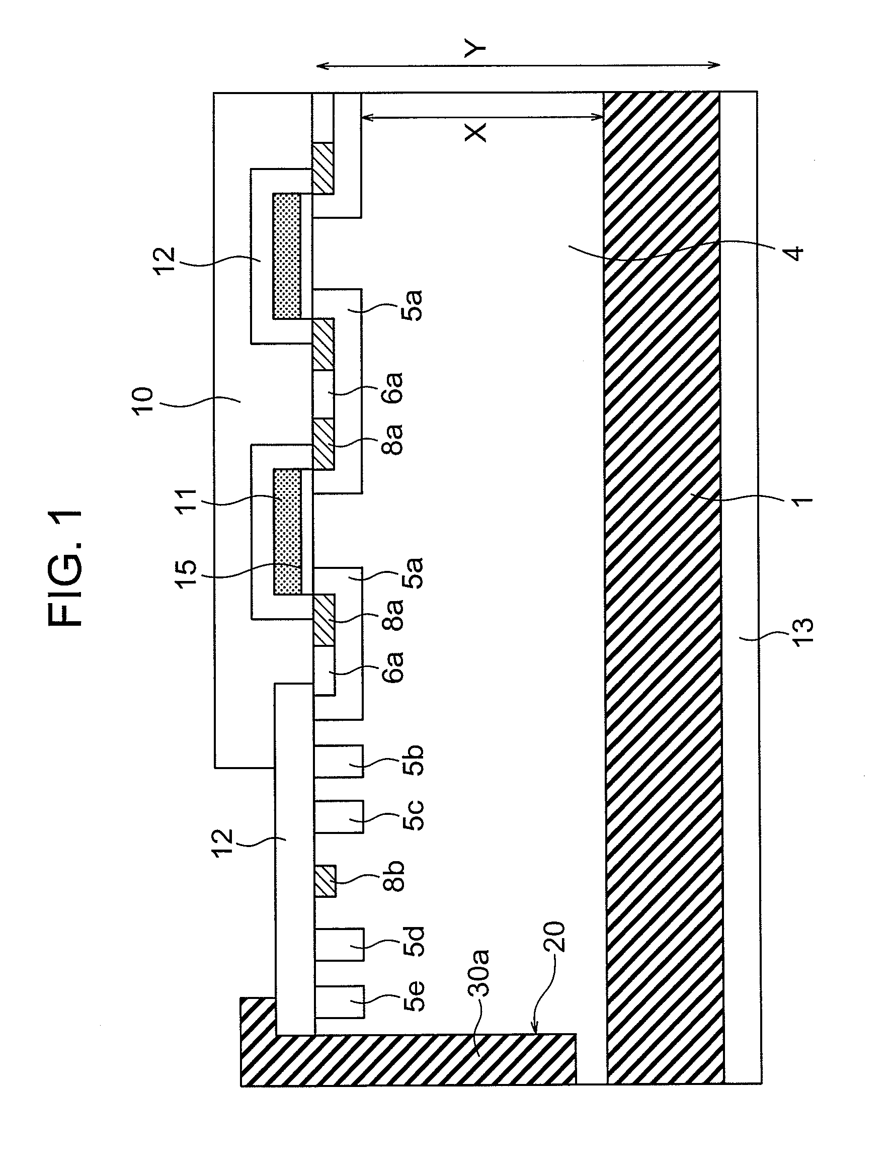
[0037]FIG. 3 indicates a semiconductor device according to an embodiment 2 of the present invention. This embodiment 2 corresponds to such a case that a silicon semiconductor region 31a formed based upon the same purpose as the silicon semiconductor region 30a of FIG. 1 is fabricated by using a polycrystal silicon layer 31 which is formed in the same step as a gate electrode layer 31 of a power MOSFET as shown in FIG. 4. It should be noted that although both the silicon semiconductor layer 31a and the gate electrode layer 11 may employ the polycrystal silicon semiconductor layer 31 formed in the same step, there is no problem even if types and concentration of the impurities are separately set. Alternatively, these layers may be formed as such polycrystal silicon layers into which the same type of impurity may be doped in high concentration.

embodiment 3

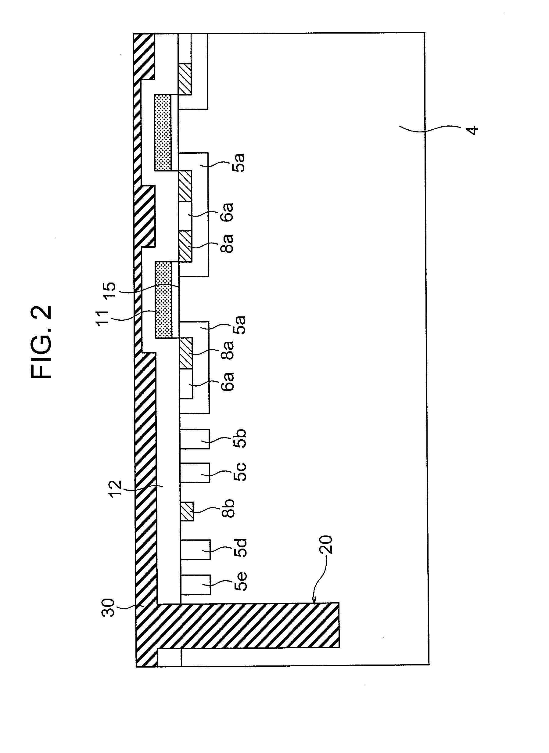
[0038]FIG. 5 indicates a semiconductor device according to an embodiment 3 of the present invention. This embodiment 3 corresponds to such a case that a silicon semiconductor region 30a is contacted to a silicon semiconductor region 1 in the semiconductor device of the embodiment 3. Even in such a case that an ohmic contact between the silicon semiconductor region 30a and the silicon semiconductor region 1 cannot be established, these two semiconductor regions 30a and 1 are connected to each other by a depletion layer which is extended from a hetero junction formed on the side of the second major plane, and is further extended from the side of the second major plane to the surface side, and when a high voltage is applied, the depletion layer is sequentially extended to the floating field rings 5e and 5d formed on the side of the major surface, so that electric field concentration in a preferable portion of the hetero junction can be avoided. As a consequence, similar to the embodime...


PUM


Abstract

A semiconductor device such as a reverse blocking type switching element is provided with a switching element made of a wide band gap semiconductor on the side of a first major plane where a first terminal is formed, while the wide band gap semiconductor is operable at a high voltage and in low loss. In a reverse blocking type switching element having a hetero junction diode for blocking a reverse direction current on the side of a second major plane where a second terminal is formed, a silicon semiconductor region is provided in a side surface of the semiconductor so as to prevent a deterioration of a withstanding voltage of the hetero junction diode.

Description

BACKGROUND OF THE INVENTION[0001]1. Field of the Invention[0002]The present invention is related to a reverse blocking type semiconductor switching element operable in low loss and having a high withstanding voltage.[0003]2. Description of the Related Art[0004]Wide band gap semiconductor elements such as SiC (silicon carbide), GaN (gallium nitride), and diamond, whose band gaps are higher than, or equal to 1.3 eV, have the following features: That is, while these wide band gap semiconductor devices can be operated in a high voltage, low loss and at a high frequency, these semiconductor device can be further operated in a high temperature. As such a semiconductor device that a wide band gap semiconductor is contacted to a silicon semiconductor, JP-A-2002-16262 (will be referred to as “patent publication 1” hereinafter) discloses a vertical type field-effect transistor which is realized by forming a GaN-series material on an Si substrate (see FIG. 1 and paragraph [0011]).[0005]On the ...

Claims


Application Information

Patent Timeline
IPC IPC(8): H01L29/74
CPCH01L21/8213H01L29/165H01L27/0605H01L29/0619H01L29/0638H01L29/0878H01L29/1602H01L29/1608H01L29/2003H01L29/42368H01L29/66068H01L29/7395H01L29/7803H01L29/7811H01L29/7816H01L21/8252
Inventor SAKAMOTO, KOZO
Owner HITACHI LTD
Why Eureka
Try Eureka