Plasma dielectric etch process including ex-situ backside polymer removal for low-dielectric constant material

a dielectric constant, exsitu backside technology, applied in the direction of photomechanical equipment, chemistry equipment and processes, instruments, etc., can solve the problems of oxidizing process doing catastrophic harm to the newer low dielectric constant insulator materials, difficult to remove all of the deposited polymer, and thinner photoresis

Inactive Publication Date: 2007-10-11
APPLIED MATERIALS INC
View PDF3 Cites 257 Cited by
  • Summary
  • Abstract
  • Description
  • Claims
  • Application Information

AI Technical Summary

Problems solved by technology

Such photoresist tends to be thinner and more prone to form imperfections such as pin holes or striations during the dielectric etch process.
However, in the post-etch polymer removal step, it is difficult to remove all of the deposited polymer.
However, such an oxidizing process does catastrophic harm to the newer low dielectric constant insulator materials such as porous carbon-doped silicon dioxide.
Another problem is that such an oxidizing process does not completely remove the backside polymer, even after 60 seconds, according to our investigation.

Method used


Image

  • Plasma dielectric etch process including ex-situ backside polymer removal for low-dielectric constant material
  • Plasma dielectric etch process including ex-situ backside polymer removal for low-dielectric constant material
  • Plasma dielectric etch process including ex-situ backside polymer removal for low-dielectric constant material

Examples


Embodiment Construction

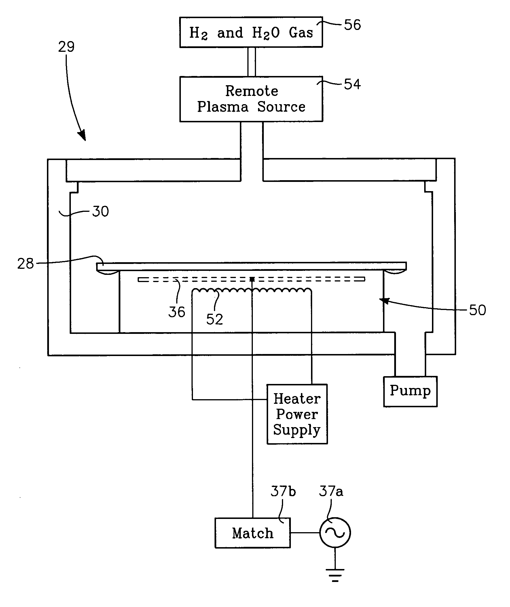
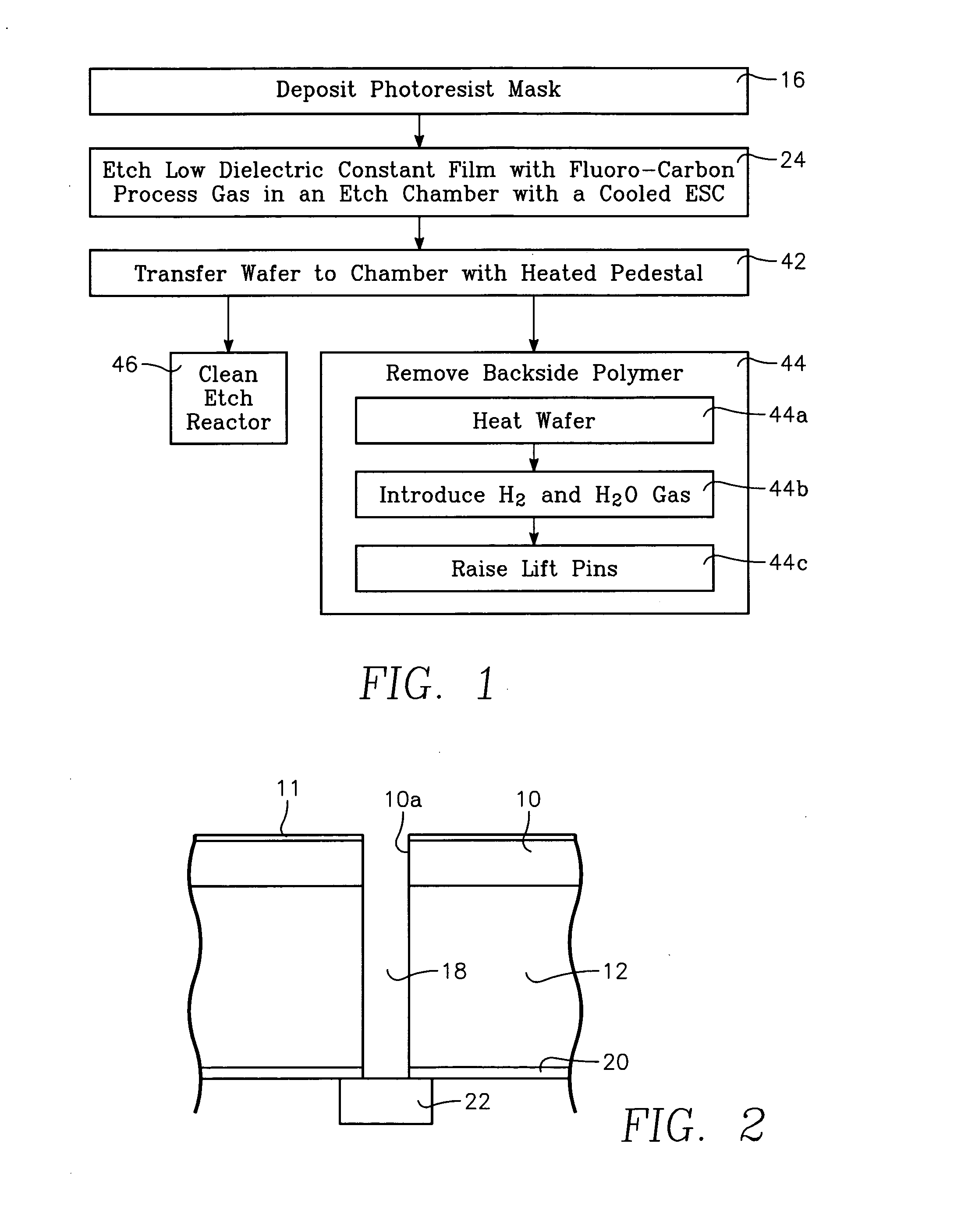
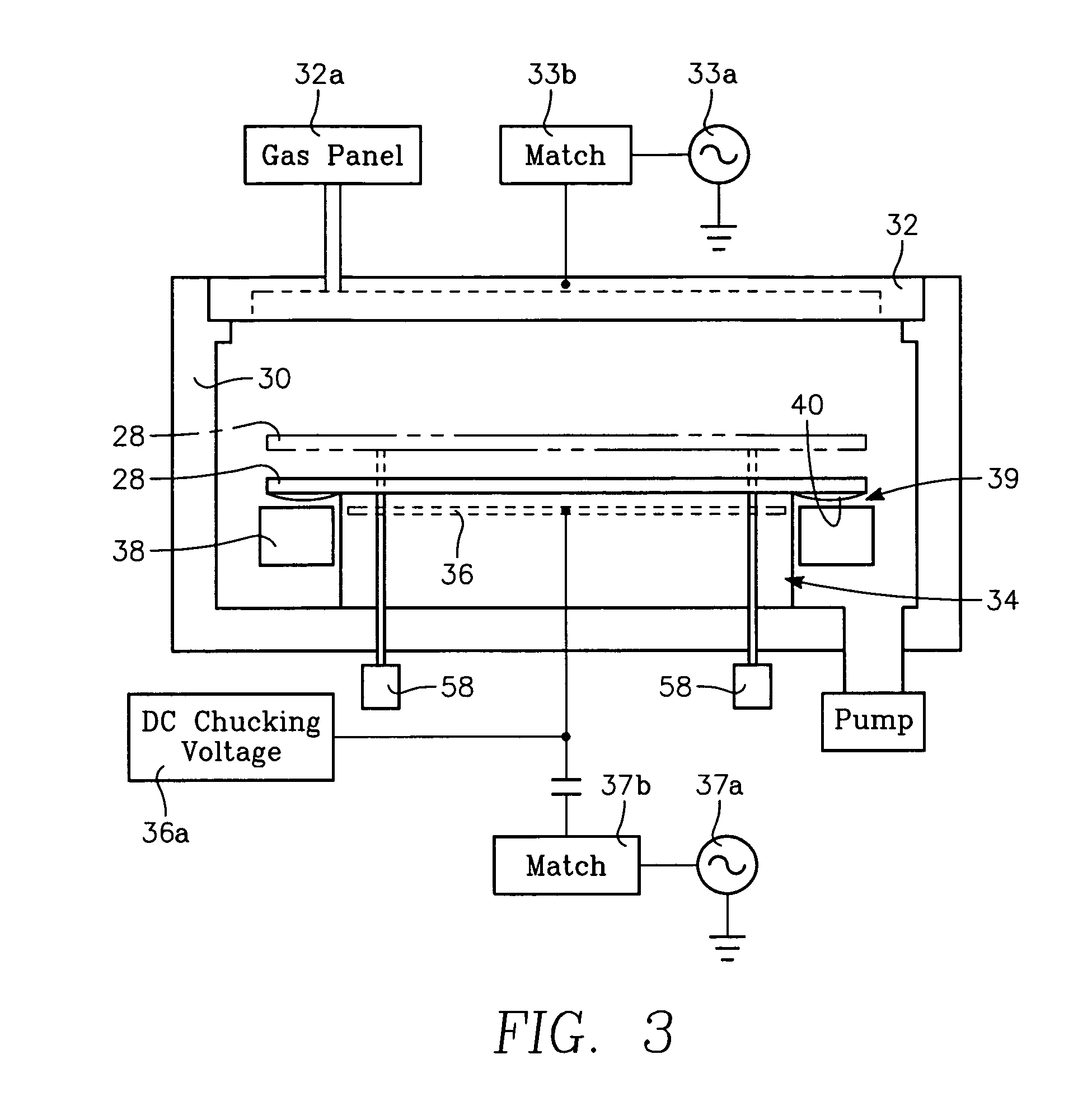
[0011] The invention is based upon our discovery of an etch process for a low dielectric constant material including a post etch polymer removal step that thoroughly removes both backside polymer and photoresist with no appreciable damage to the low dielectric constant insulator layer (e.g., porous carbon-doped silicon dioxide or a porous organo-silicate material), and does so in less than 60 seconds. An etch process embodying the invention is depicted in FIG. 1, while FIG. 2 depicts one example of a thin film structure that can be formed using the process of FIG. 1. A photoresist mask 10 depicted in FIG. 2 is deposited on a dielectric layer 12, the mask 10 having an aperture 10a corresponding to a feature 18 that is to be etched in the dielectric layer 12. This corresponds to the step of block 16 of FIG. 1. The feature may be a narrow via 18. The via 18 extends through the dielectric layer 12 and through a barrier layer 20 to expose the top surface of a copper line 22. The dielectr...


PUM

PropertyMeasurementUnit
period of timeaaaaaaaaaa
timeaaaaaaaaaa
pressureaaaaaaaaaa

Abstract

A plasma etch process for etching a porous carbon-doped silicon oxide dielectric layer using a photoresist mask is carried out first in an etch reactor by performing a fluorocarbon based etch process on the workpiece to etch exposed portions of the dielectric layer while depositing protective fluorocarbon polymer on the photoresist mask. Then, in an ashing reactor, polymer and photoresist are removed by heating the workpiece to over 100 degrees C., exposing a peripheral portion of the backside of said workpiece, and providing products from a plasma of a hydrogen process gas to reduce carbon contained in polymer and photoresist on said workpiece until the polymer has been removed from a backside of said workpiece. The process gas preferably contains both hydrogen gas and water vapor, although the primary constituent is hydrogen gas. The wafer (workpiece) backside may be exposed by extending the wafer lift pins.

Description

BACKGROUND OF THE INVENTION [0001] Integrated circuit performance is being continually improved by increasing device switching speed, increasing interconnection density and reducing cross-talk between adjacent conductors. Switching speeds have been increased and cross-talk reduced by employing new dielectric thin film material having low dielectric constant, such as porous carbon-doped silicon dioxide. Interconnections have been increased by increasing the number of interconnected conductive layers and reducing feature size (e.g., line widths, hole diameters). Connecting between such deep layers entails high aspect ratio (deep and narrow) conductor openings or “vias”. Such fine features have required photoresist (for photolithography) adaptable to shorter wavelengths. Such photoresist tends to be thinner and more prone to form imperfections such as pin holes or striations during the dielectric etch process. This problem is addressed by employing a fluorocarbon chemistry during the p...

Claims


Application Information

Patent Timeline
Patent Type & Authority Applications(United States)
IPC IPC(8): H01L21/302H01L21/461
CPCG03F7/427H01L21/31138H01L21/0209H01J37/32357H01L21/3065
Inventor DELGADINO, GERARDO A.LAHIRI, INDRAJITSU, TEH-TIENSHEIH, BRIAN SY-YUANSINHA, ASHOK K.
Owner APPLIED MATERIALS INC
Why Eureka
Try Eureka