Fluorene compound and organic light-emitting device using the compound
- Summary
- Abstract
- Description
- Claims
- Application Information
AI Technical Summary
Benefits of technology
Problems solved by technology
Method used
Image
Examples
example 1
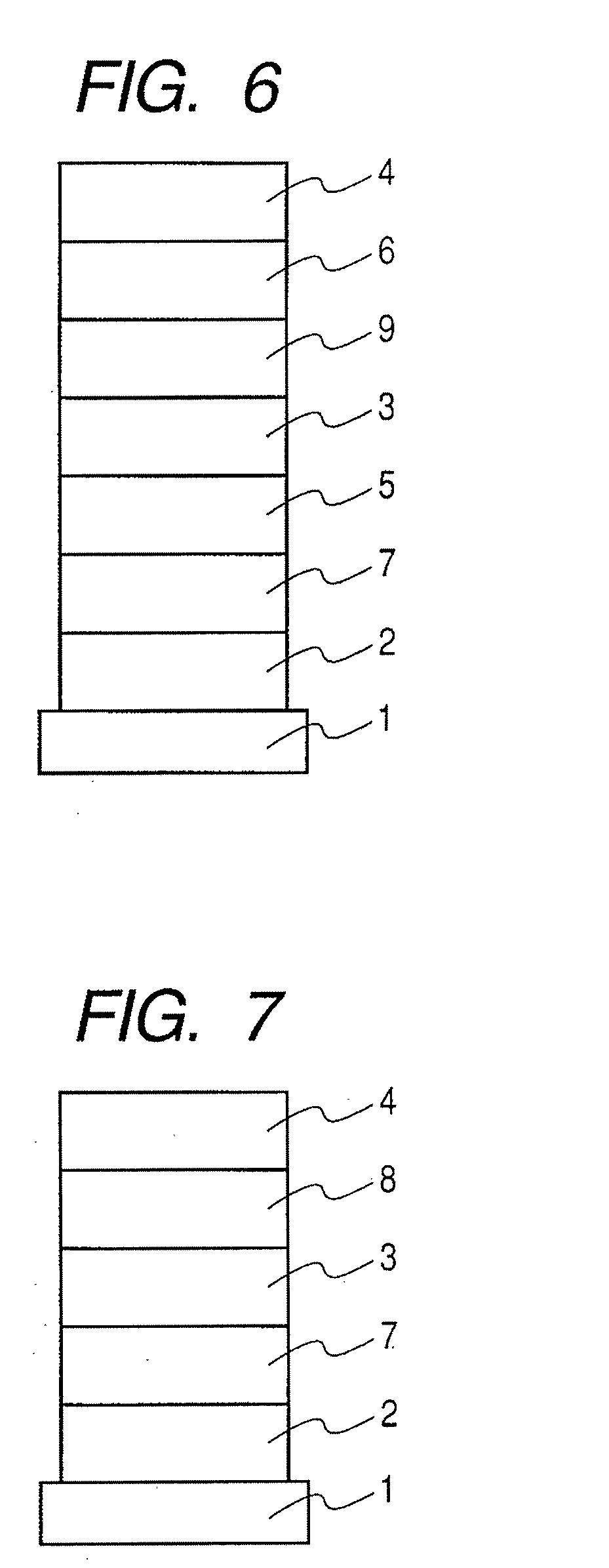
[0120]A device with the structure shown in FIG. 7 was produced.
[0121]A transparent conductive support substrate was prepared which had a film of indium tin oxide (ITO) with a thickness of 120 nm as the anode 2 formed on a glass plate as the substrate 1 by a sputtering method. The transparent conductive support substrate was ultrasonically cleaned sequentially with acetone and isopropyl alcohol (IPA), subsequently washed with boiled IPA, was then dried, was further cleaned with UV / ozone, and was used.
[0122]On the transparent conductive support substrate, a film of poly(3,4-ethylenedioxythiophene) (Baytron P AI-4083 (trade name); manufactured by Bayer) was made in a thickness of 50 nm by spin coating to form the hole injection layer 7.
[0123]Further, a film was made in a thickness of 60 nm by spin coating of a 2 wt. % toluene solution of Exemplary Compound No. 11 to form the light-emitting layer.
[0124]Next, as the electron injection layer 8, calcium was used to form a metal layer film ...
examples 2-3 and 5-20
[0129]Devices were produced by following the same procedure as in Example 1 with the exception that the exemplified compounds shown in Table 1 were used in place of Exemplified Compound No. 11 used in Example 1, and the same evaluation as in Example 1 was performed thereto. The results are shown in Table 1.
example 21
[0131]A device was produced by following the same procedure as in Example 1 with the exception that a film with a thickness of 60 nm was made by spin coating of a toluene solution which contained 0.2 wt. % of the Ir complex represented by the following structural formula and 2 wt. % of Exemplary Compound No. 4 to thereby form the light-emitting layer 3.
[0132]When a DC voltage of 5 V was applied to the thus obtained device with the ITO electrode (anode 2) being connected to a positive electrode and the Al electrode (cathode 4) being connected to a negative electrode, a current flowed through the device at a current density of 20 mA / cm2 and emission of a green light was observed with a luminance of 1,600 cd / m2.
[0133]Furthermore, when a voltage was applied to the device for 50 hours so that the current density was kept at 5.0 mA / cm2, the device emitted light at a luminance of 600 cd / m2 in an early stage and at 520 cd / m2 after the elapse of the 50 hours, which meant that the luminance d...
PUM
| Property | Measurement | Unit |
|---|---|---|
| Electric potential / voltage | aaaaa | aaaaa |
| Current density | aaaaa | aaaaa |
| Current density | aaaaa | aaaaa |
Abstract
Description
Claims
Application Information


