[0155]It should be noted that in
flash memory chips, the convention has been to use the same floating
gate oxide that is used between the floating gate and the channel for the
gate oxide of low, and some medium
voltage transistors in order to save extra process steps. Therefore the conventional tunnel
oxide with a thickness that is usually greater than 8 nm has been limiting the performance, sub-threshold slope, and on-current drive of the low and some medium
voltage transistors. This has resulted in slower program, and read characteristics. One
advantage of the present invention is to provide a
peripheral transistor gate oxide that is electrically and effectively much thinner than the conventional tunnel
oxide, and is physically thicker than the conventional tunnel oxide. In other words, the
peripheral circuitry will benefit from replacing the conventional tunnel oxide gate with high-K material(s) in alignment with the general trend of the
semiconductor industry towards high-K materials.
[0156]Step 1202 of FIG. 25 includes performing implants and associated anneals of the triple well. The result of step 1202 is depicted in FIG. 26A, which depicts P substrate 1018, N-well 1022 within P-substrate 1018, and P-Well 1020 within N-well 1022. The sidewalls of the N-well that isolate the P-wells from one another are not depicted. Also the N-well depth is typically much thicker than that of the P-well in contrast to FIG. 26A. The P substrate is usually the thickest consisting of the majority of the
wafer thickness. In step 1204, the high-K material(s) is deposited on top of P-Well 1020. The high-K material may be deposited using Atomic Layer Deposition (ALD) in accordance with various embodiments as described herein. Additionally (and optionally), other materials may be deposited on, deposited under or incorporated within the high-K material in order to form
dielectric layer 1030. The result of step 1204 is depicted in FIG. 26B, which shows
dielectric layer 1030, with the high-K material. Note that one
advantage of using the high-K material in the lower
dielectric layer is that it can also be used for
low voltage peripheral transistors to increase performance.
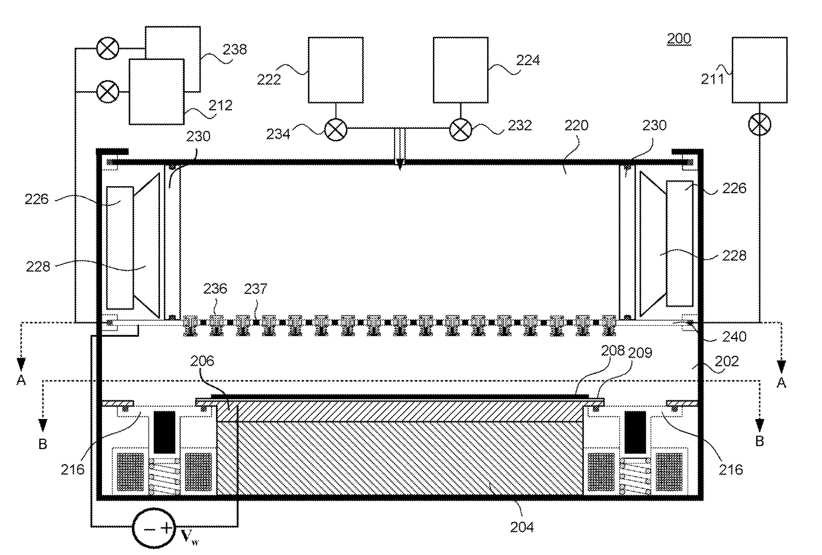
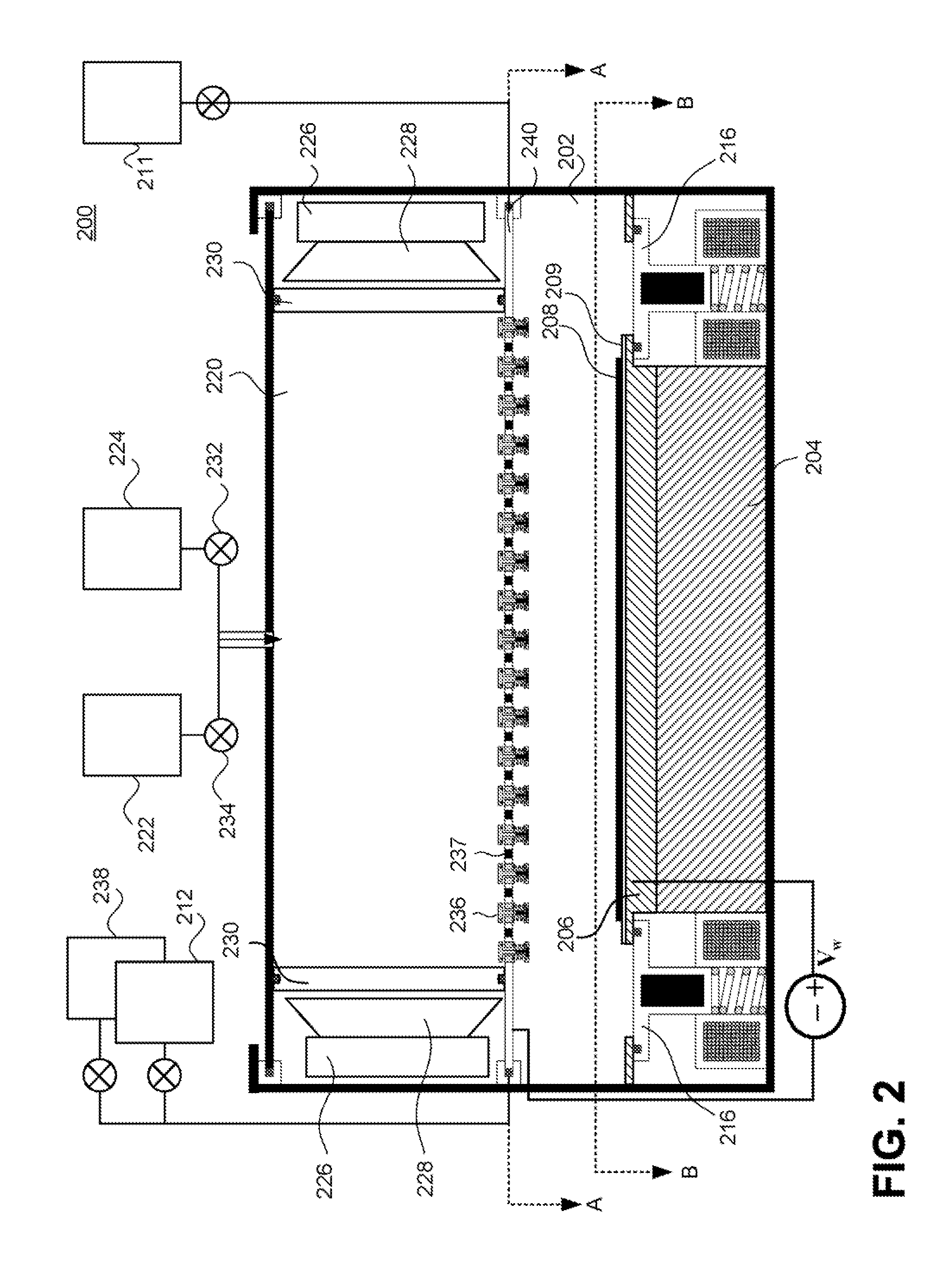
[0157]In accordance with one embodiment, step 1204 can include the deposition of a high-K material using one or more of the techniques as preiously described. For example, a high-density
plasma deposition system can be used that utilizes a Kr feed gas in combination with a
plasma chamber bias,
wafer bias, selectively permeable membrane, and / or additional particle dissociating
energy source to deposit an oxide,
nitride, oxynitride or other suitable high-K material. In one embodiment, the high-K material can be flash heated after one or more deposition cycles to release contaminant incorporation in the substrate. As previously described, the effective thickness of the dielectric region between the channel and the floating gate should be reduced in order to maintain control of the floating gate over the channel. An ALD process incorporating Kr as an
ion generating feed gas to provide high radical concentrations facilitates the deposition of a high quality dielectric having a high dielectric constant. The low thermal ALD process will minimize the
diffusion of dopants, stop the poly-
crystallization of the dielectric material, and minimize the inter-
diffusion of
silicon atoms into the material.
[0158]In accordance with various embodiments, the deposition of a high-K material at step 1204 can include the simultaneous growth of one or more interfacial
layers using a high radical concentration. Interfacial
layers are undesirable in typical applications, as previously discussed, given that their dielectric constant tends to be substantially lower than the dielectric constant of the high-K material. In accordance with various embodiments of the present invention, however, these interfacial
layers can be beneficial, and hence, a high radical concentration is achieved to facilitate the growth of lower dielectric constant interfacial layers while performing a
deposition process. While a grown interfacial layer such as SiO2 may have a lower dielectric constant, it also has a higher energy barrier (ΔEc), that reduces the possibility of
electron injection into the high-K dielectric by both direct tunneling and Fowler-Nordheim tunneling. Because a storage element in accordance with embodiments is programmed by transferring a charge from the control gate across the inter poly dielectric to the floating gate, a barrier to tunneling from the channel is very beneficial. This is in contrast to typical storage elements where tunneling across the
dielectric layer separating the channel from the floating gate is achieved to program and erase the
cell.
[0159]A high-density plasma source chamber utilizing one or more techniques as previously described can be used in one embodiment to increase the radical concentration delivered to the reacting surface for deposition. Some of the highly reactive radicals (e.g., oxygen) can penetrate the high-K dielectric being deposited and react with the underlying
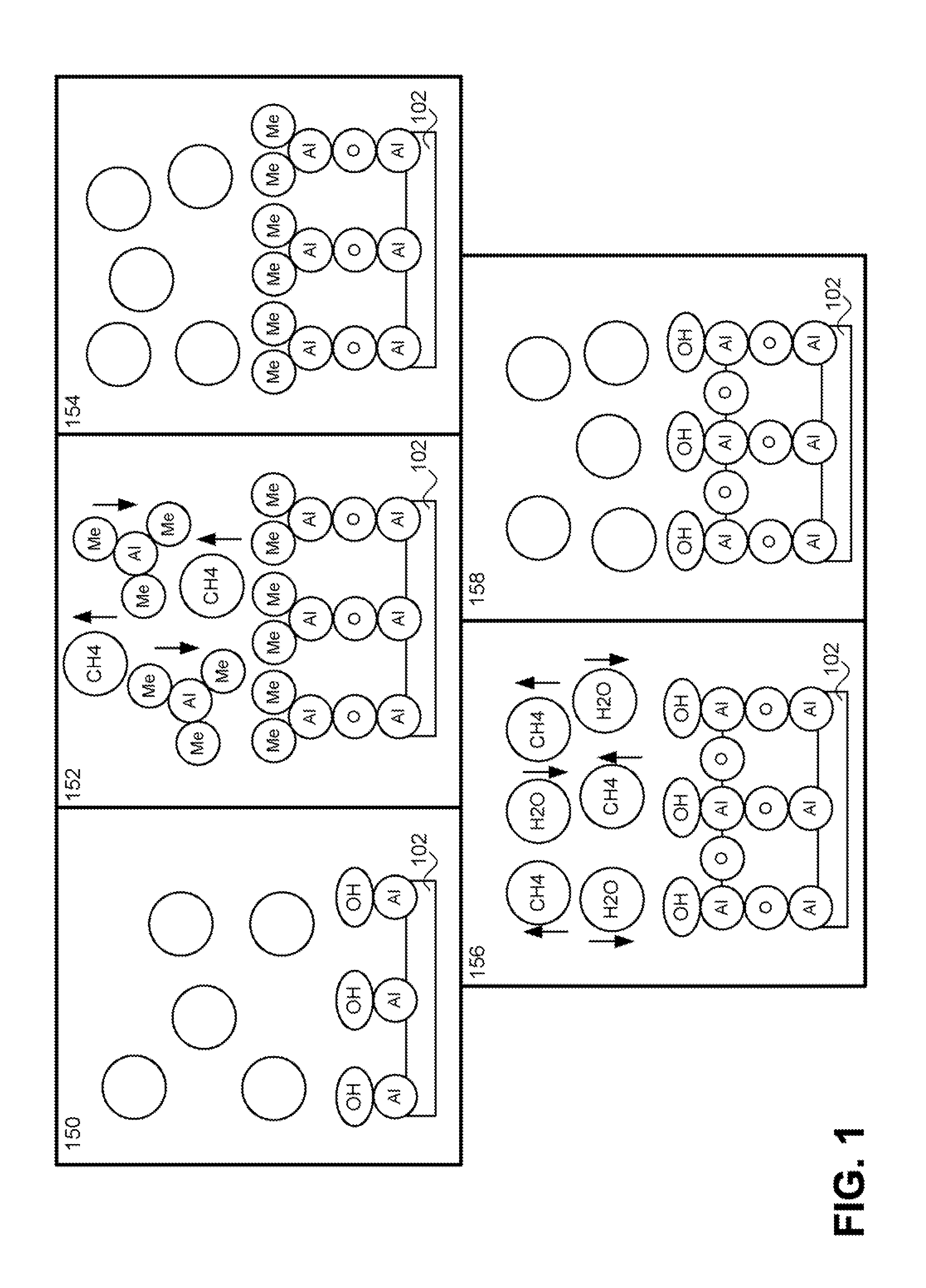
silicon substrate to grow one or more interfacial layers. These interfacial layers are grown in addition to the material being deposited. For example, an Al2O3 high-K material may be deposited while one or more lower-K SiO2 interfacial layers are grown from the
silicon based substrate. After the Al containing first precursor is introduced, adsorbed, and purged from the
deposition chamber, oxygen radicals can be generated from a high-density plasma source and introduced to the
deposition chamber, along with Kr ions, to react at the
substrate surface and form a
monolayer of Al2O3. Some of the oxygen radicals will reach the silicon substrate and cause the growth of SiO2.
[0160]The aforementioned simultaneous growth and deposition technique can be used when depositing any film where it is desired o produce such interfacial layers. The technique need not be practiced in conjunction with the
storage cell presented herein.

