TFT array substrate and method of manufacturing the same

a technology of array substrate and substrate, which is applied in the field of tft array substrate, can solve the problems of reducing the mobility of tft, hindering the achievement of large-size tft-lcd, high-definition and high-speed response, and the inability to establish a direct contact between al and nsup>+/sup>a-si, so as to improve the coverage characteristics of the gate and improve the heat resistance

Active Publication Date: 2007-12-27
TRIVALE TECH
View PDF5 Cites 14 Cited by
  • Summary
  • Abstract
  • Description
  • Claims
  • Application Information

AI Technical Summary

Benefits of technology

[0055]In this embodiment, an alloy film which made of Al with 6 wt % of Ni addition is used as the first and second metal thin films. Adding Ni to Al achieves good electric contact characteristics between the second metal thin film and an n+a-Si film to form the ohmic contact film 8. It also achieves good electric contact characteristics between the first and second metal thin films and the ITO film. The additive amount of Ni is not limited to 6 wt %, and the preferred range is from 1.0 wt % to 30 wt %. The addition of Ni of 1.0 wt % or higher allows the suppression of mutual diffusion of Si elements at the interface between the second metal thin film and the n+a-Si film. This also allows the suppression of mutual diffusion of O elements at the interface between the first and second metal thin films and the ITO film. It is thereby possible to obtain good electric contact characteristics. On the other hand, if the additive amount of Ni exceeds 30 wt %, the electric specific resistance becomes 20 μΩ cm or higher. This loses the advantage over conventional Cr (specific resistance: 20 μΩ cm), Ti (specific resistance: 50 μΩ cm) and Ta (specific resistance: 25 μΩ cm). The specific resistance can be within the range of 3.5 to 20 μΩ cm by limiting the additive amount of Ni to the range of 1.0 wt % to 30 wt %, thus achieving the low resistance lines, which are an advantage of the present invention.
[0056]Further, a rare-earth element such as Y, La or Nd may be added to the AlNi alloy. The addition of the rare-earth element allows the improvement of heat resistance. For example, it is possible to prevent the occurrence of hillock, which is projecting surface roughness, in spite of the annealing process at the temperature of 200° C. to 230° C. This improve the coverage characteristics of the gate insulating film 6 above the gate electrode 2, the gate line 3, the auxiliary capacitor electrode 4 and the gate terminal 5, and the passivation film 14 above the source electrode 9, the source line 10 and the drain electrode 11. The additive amount of the rare-earth element may be optimized so that the effect of suppressing hillock and the electric specific resistance are within a desired range.Second Embodiment
[0057]The TFT array substrate according to a second embodiment of the present invention is used for electro-optic displays, and a liquid crystal display is described hereinbelow as an example. The top plan view and the cross-sectional view of the TFT array substrate are the same as those in the first embodiment shown in FIGS. 2 and 3. The structure of the TFT array substrate is the same as that of the first embodiment except for the material of the first and second metal thin films, and the description is not repeated herein. In this embodiment, an alloy film composed mainly of Mo or a pure Mo film is used as the first and second metal thin films. Thus, the gate electrode 2, the gate line 3, the auxiliary capacitor electrode 4, the gate terminal 5, the source electrode 9, the source line 10, the drain electrode 11 and the source terminal 12 are made of an alloy film composed mainly of Mo or a pure Mo film.
[0058]A method of manufacturing the TFT array substrate of the liquid crystal display according to this embodiment is described hereinafter with reference to FIG. 4. As described earlier, this embodiment is the same as the first embodiment except for the first and second metal thin films and thus not described in detail herein.
[0059]First, the gate electrode 2, the gate line 3, the auxiliary capacitor electrode 4, and the gate terminal 5 are formed. In a preferred embodiment, an alloy film composed mainly of Mo is used as the first metal thin film. Specifically, it is a MoNb alloy film containing Mo with 5 wt % of Nb addition. The MoNb alloy film is deposited at the thickness of 200 nm by sputtering using known Ar gas. In the sputtering, an alloy target of Mo with Nb addition is used. The sputtering conditions, the etching method and so on are the same as those in the first embodiment. The gate electrode 2, the gate line 3, the auxiliary capacitor electrode 4, and the gate terminal 5 are thereby formed. The first metal thin film may be a pure Mo film. In this process, the pattern of the first metal thin film is formed on the transparent insulating substrate 1 as shown in the column (a) of FIG. 4.
[0060]Next, the gate insulating film 6, the semiconductor film 7 and the ohmic contact film 8 are deposited sequentially by CVD process such as plasma CVD. The second photolithography process is then performed to form the pattern of the semiconductor film 7 and the ohmic contact film 8. The structure shown in the column (b) of FIG. 4 is thereby formed on the transparent insulating substrate 1.

Problems solved by technology

However, this causes a decrease in the mobility of TFT.
Further, the high line resistance hinders the achievement of a large-size TFT-LCD, high-definition and high-speed response.
In this structure, however, it is impossible to establish a direct contact between Al and n+a-Si and a direct contact between Al and an ITO.
Thus, a direct contact between the SD and an ohmic contact film and a direct contact between the SD and a transparent pixel electrode cannot be established in this structure.
In this method, however, it is necessary to deposit three layers for the SD, which complicates the production process.

Method used


Image

  • TFT array substrate and method of manufacturing the same
  • TFT array substrate and method of manufacturing the same
  • TFT array substrate and method of manufacturing the same

Examples


first embodiment

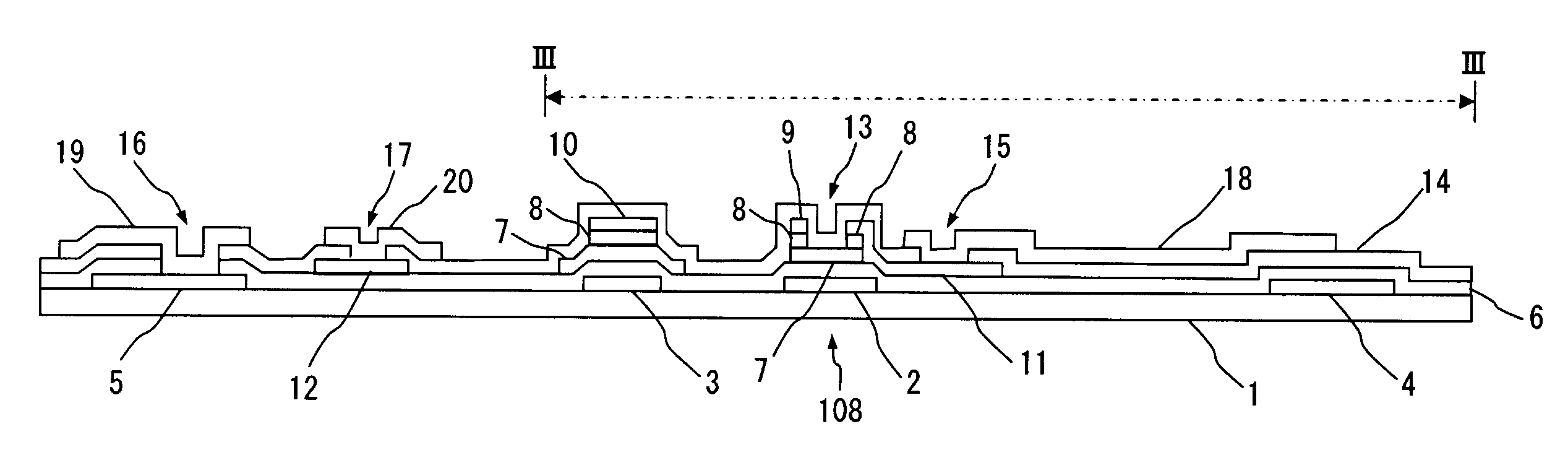
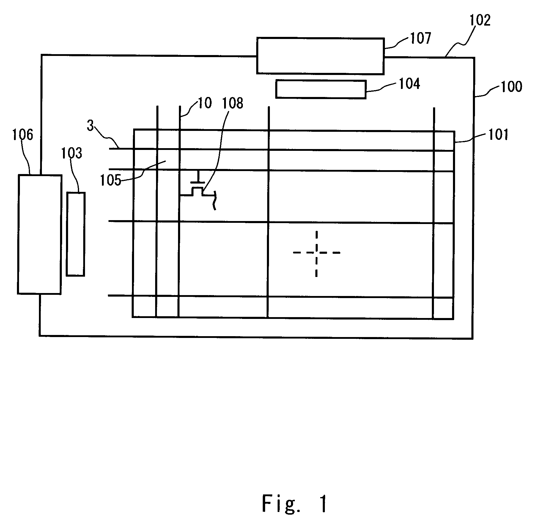
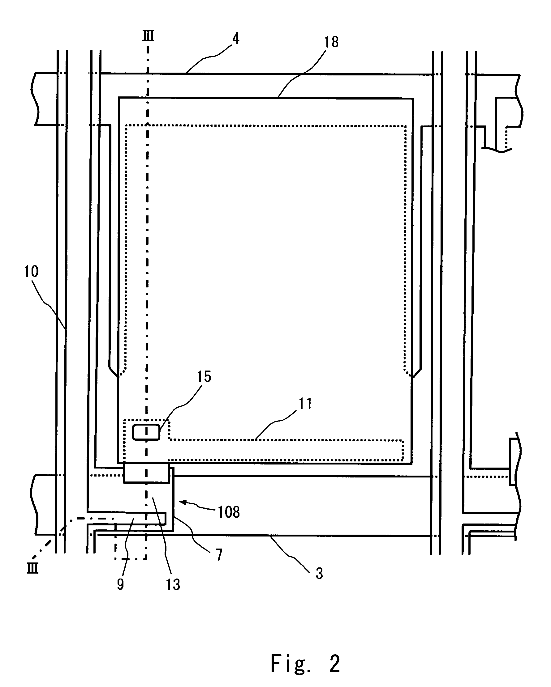
[0026]The structure and manufacturing method of a TFT array substrate according to a first embodiment of the present invention are described hereinafter with reference to the drawings. FIG. 2 is a top plan view showing the structure of a pixel of a TFT array substrate according to this embodiment, and FIG. 3 is a cross-sectional view along line III-III in FIG. 2. FIG. 3 further shows a gate terminal portion and a source terminal portion on the left part thereof. The TFT array substrate of this embodiment is used for electro-optic displays, and a liquid crystal display is described hereinbelow as an example.

[0027]A gate electrode 2, a gate line 3, an auxiliary capacitor electrode 4, and a gate terminal 5 are formed on a transparent insulating substrate 1, which is made of glass or the like. The gate line 3 includes the gate electrode 2, and the gate terminal 5 exists at an end of the gate line 3. The gate electrode 2 constitutes a TFT 108, which serves as a switching device. The auxi...

second embodiment

[0057]The TFT array substrate according to a second embodiment of the present invention is used for electro-optic displays, and a liquid crystal display is described hereinbelow as an example. The top plan view and the cross-sectional view of the TFT array substrate are the same as those in the first embodiment shown in FIGS. 2 and 3. The structure of the TFT array substrate is the same as that of the first embodiment except for the material of the first and second metal thin films, and the description is not repeated herein. In this embodiment, an alloy film composed mainly of Mo or a pure Mo film is used as the first and second metal thin films. Thus, the gate electrode 2, the gate line 3, the auxiliary capacitor electrode 4, the gate terminal 5, the source electrode 9, the source line 10, the drain electrode 11 and the source terminal 12 are made of an alloy film composed mainly of Mo or a pure Mo film.

[0058]A method of manufacturing the TFT array substrate of the liquid crystal ...


PUM

PropertyMeasurementUnit
temperatureaaaaaaaaaa
thicknessaaaaaaaaaa
thicknessaaaaaaaaaa

Abstract

A TFT array substrate includes a TFT having an ohmic contact film and a source electrode and a drain electrode formed on the ohmic contact film. It also includes a pixel electrode electrically connected with the drain electrode. The source electrode and the drain electrode are made of an Al alloy containing Ni as an additive.

Description

BACKGROUND OF THE INVENTION[0001]1. Field of the Invention[0002]The present invention relates to a TFT array substrate and a method of manufacturing the same.[0003]2. Description of Related Art[0004]An electro-optic device such as a liquid crystal display attracts attention as one of flat panel displays to replace CRT. It has the features of low power consumption and thin profile and is widely applied to products having such features. An active matrix liquid crystal display often uses a TFT as a switching device.[0005]In order to improve the productivity of such a liquid crystal display, it is necessary to reduce the number of manufacturing steps of a TFT array substrate having TFTs. For example, a manufacturing method that reduces the number of photolithography steps is disclosed in Japanese Unexamined Patent Application Publication No. 8-50308 (paragraphs 0084-0089, FIGS. 54 to 63). This technique allows the production of a TFT array substrate in five photolithography steps.[0006]...

Claims


Application Information

Patent Timeline
Patent Type & Authority Applications(United States)
IPC IPC(8): H01L29/04
CPCH01L27/12H01L29/458H01L29/4908H01L27/124H01L27/1214
Inventor YANO, SHINICHINAKAHORI, TADAKIISHIGA, NOBUAKI
Owner TRIVALE TECH
Why Eureka
Try Eureka