Carrier-suppressed optical pulse train generation method and mode-locked semiconductor laser diode for realizing this method

a carrier-suppressed optical pulse and laser diode technology, applied in the direction of optical resonator shape and construction, instrumentation, laser details, etc., can solve the problems of large device for realizing the first method, high power consumption of the first method, and inability to achieve a wide spectrum of optical pulse signals

Inactive Publication Date: 2008-01-31
OKI ELECTRIC IND CO LTD
View PDF14 Cites 37 Cited by
  • Summary
  • Abstract
  • Description
  • Claims
  • Application Information

AI Technical Summary

Benefits of technology

[0070]In step C1, modulating the transmittance of the optical modulation region at the frequency frep makes it possible to put the first distributed Bragg reflector semiconductor laser under mode-locked operation. That is, it becomes a state in which a fixed correlation is introduced among the oscillation longitudinal modes. Oscillating the first distributed Bragg reflector semiconductor laser in a state that maintains a fixed correlation among oscillation longitudinal modes makes it possible to output an optical pulse train with a repetitive frequency of frep. The second CS optical pulse train generation method is realized by a second distributed Bragg reflector semiconductor laser as follows. The second CS optical pulse train generation method, similar to the first CS optical pulse train generation method, is also a method for generating a CS optical pulse train with a repetitive frequency of frep by putting a second distributed Bragg reflector semiconductor laser under mode-locked operation at an oscillation longitudinal mode applied at f0±q(frep/2).
[0071]The point of difference with the first CS optical pulse train generation method is the incorporation of step D2, which sets the value of an optical absorption coefficient of the optical absorption coefficient adjustment region to a size sufficient to prevent reflected light from the cavity facet of the side of the optical absorption coefficient adjustment region ...

Problems solved by technology

In either case, an optical pulse signal having a wide spectrum band is not desirable from the standpoint of efficiently utilizing the frequency band of an optical communications network in which this optical pulse signal is being used.
However, because the first method requires a CW light source in addition to the LN optical intensity modulator, a device for realizing the first method will be large.
This makes the impedance of the LN optical intensity modulator 50Ω, which, if converted...

Method used


Image

  • Carrier-suppressed optical pulse train generation method and mode-locked semiconductor laser diode for realizing this method
  • Carrier-suppressed optical pulse train generation method and mode-locked semiconductor laser diode for realizing this method
  • Carrier-suppressed optical pulse train generation method and mode-locked semiconductor laser diode for realizing this method

Examples


first embodiment

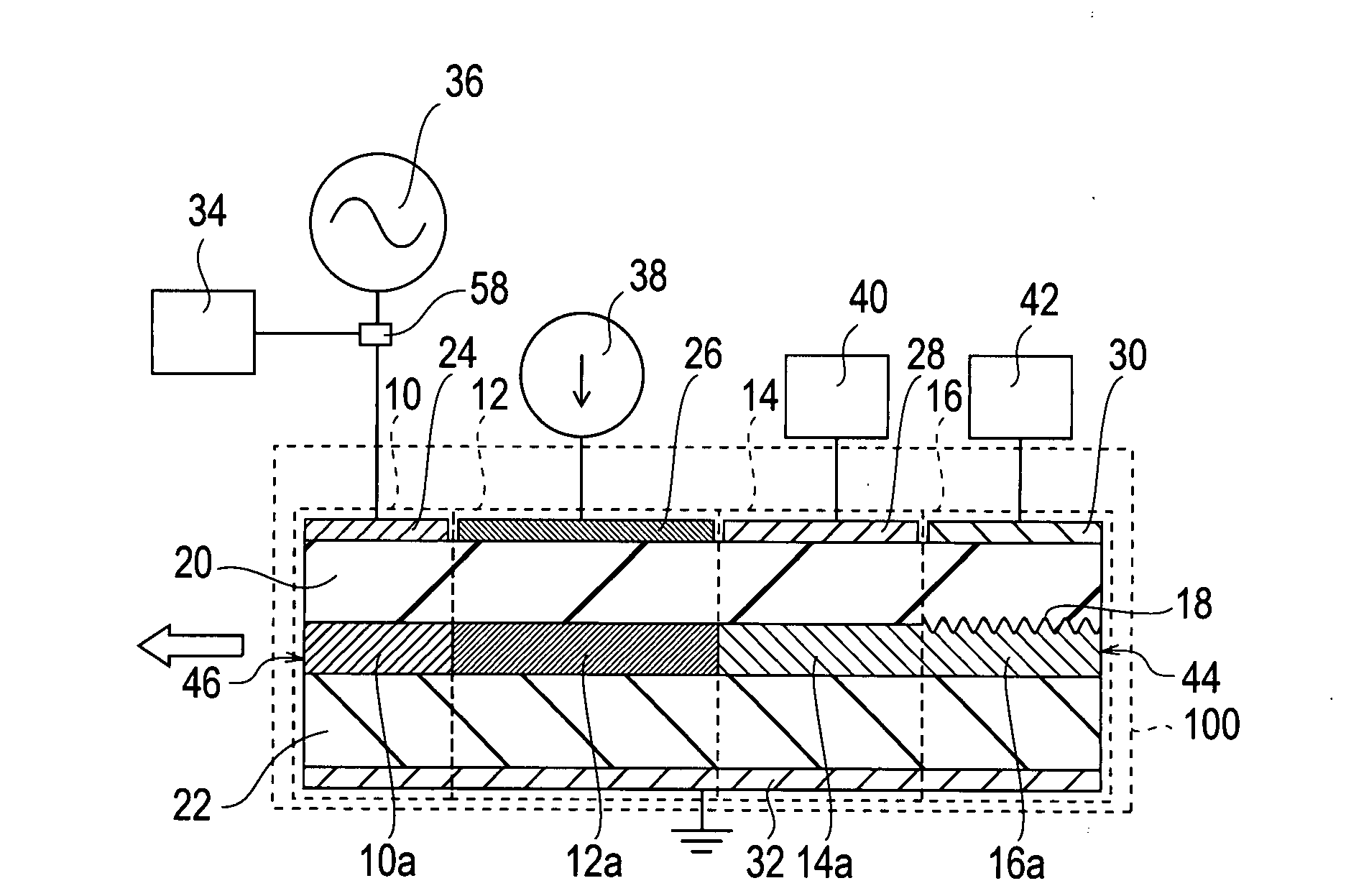
[0097]The constitution of a first distributed Bragg reflector semiconductor laser for realizing a first CS optical pulse train generation method will be explained by referring to FIG. 1A and FIG. 1B. Further, the mode-locked operating principle of this first distributed Bragg reflector semiconductor laser will also be explained. FIG. 1A and FIG. 1B are both diagrams for explaining a first mode-locked semiconductor laser diode, that is, diagrams for explained a simplified structure of a distributed Bragg reflector semiconductor laser for realizing a first CS optical pulse train generation method.

[0098]FIG. 1A shows an enlarged cross-sectional view of a distributed Bragg reflector semiconductor laser for realizing changes to the effective indices of the optical waveguides of a phase control region and a distributed Bragg reflector region by virtue of the plasma effect or the Pockels effect. Further, FIG. 1B shows an enlarged cross-sectional view of a distributed Bragg reflector semico...

second embodiment

[0180]The constitution of a distributed Bragg reflector semiconductor laser 300, which is a second distributed Bragg reflector semiconductor laser for realizing a second CS optical pulse train generation method, will be explained by referring to FIG. 11. The mode-locked operation principle of this distributed Bragg reflector semiconductor laser 300 will also be explained. FIG. 11 is a simplified enlarged cross-sectional view of the distributed Bragg reflector semiconductor laser 300 for realizing a second CS optical pulse train generation method.

[0181]The distributed Bragg reflector semiconductor laser 300 differs from distributed Bragg reflector semiconductor lasers 100 and 200 in that an optical absorption coefficient adjustment region 60 is also integrated into the cavity facet side of the distributed Bragg reflector region 16. The constitution of the parts other than this is the same as that of distributed Bragg reflector semiconductor lasers 100 and 200 shown in FIG. 1A and FIG...

third embodiment

[0214]The constitution of a Fabry-Perot external-cavity type semiconductor laser 400 used in a third CS optical pulse train generation method will be explained by referring to FIG. 16. FIG. 16 is a simplified enlarged cross-sectional view for illustrating the constitution of a Fabry-Perot external-cavity type semiconductor laser 400 of a third embodiment. The Fabry-Perot external-cavity type semiconductor laser 400 is constituted comprising a wavelength filter 68, which converts a center transmission wavelength to a frequency f0, and a multi-electrode semiconductor laser diode element 500, which is constituted by linearly arranging an optical modulation region 10 comprising a function for modulating optical intensity, and a gain region 12, in which population inversion is achieved. This wavelength filter 68 and this multi-electrode semiconductor laser diode element 500 are arranged linearly and housed in an external cavity.

[0215]More specifically, the Fabry-Perot external-cavity typ...


PUM


Abstract

A CS optical pulse train generation method, which is able to change the half width of an optical pulse constituting a CS optical pulse train, and which is compact and has low power consumption. A distributed Bragg reflector semiconductor laser utilized in this method is one which is constituted comprising an optical modulation region, a gain region, a phase control region, and a distributed Bragg reflector region. Current is injected into the gain region by way of a p-side electrode and a n-side common electrode by a constant current source, forming the population inversion required for laser oscillation. Optical modulation required to manifest mode locking is carried out in the optical modulation region. A diffraction grating is formed in the distributed Bragg reflector region. A CS optical pulse train with a repetitive frequency of frep is generated by adjusting the effective indices of both the phase control region and the distributed Bragg reflector region such that, of the longitudinal modes of the mode-locked semiconductor laser diode, the two longitudinal modes close to the frequency f0, which is the Bragg wavelength of the distributed Bragg reflector region converted to a frequency, become f0+(frep/2) and f0−(frep/2).

Description

BACKGROUND OF THE INVENTION[0001]1. Field of the Invention[0002]The present invention relates to a method for generating a carrier-suppressed optical pulse train and a mode-locked semiconductor laser diode for realizing this method, for generating an optical pulse signal using the intensity modulation of a carrier-suppressed-Return to Zero format.[0003]2. Description of Related Art[0004]Optical communications networks are being improved to transmit information over greater distances and to provide increased capacity. A variety of formats have been proposed for the optical signals used in an optical communications system constituting an optical communications network, and a number of these optical signal formats have been commercialized. A typical commercial optical signal format is the intensity modulation format, which expresses a binary digital signal by strengthening and weakening optical intensity. This intensity modulation format can be broadly divided into two types: the NRZ (...

Claims


Application Information

Patent Timeline
IPC IPC(8): H01S3/0941G02F1/01
CPCH01S5/0265H01S5/0657H01S5/06256H01S5/06246
Inventor ARAHIRA, SHIN
Owner OKI ELECTRIC IND CO LTD
Why Eureka
Try Eureka