Method for manufacturing a semiconductor device including a stacked capacitor

a technology of stacked capacitors and semiconductor devices, which is applied in the direction of capacitors, basic electric elements, electrical appliances, etc., can solve the problems of preventing the improvement of capacitor insulation films for achieving higher capacitance, and achieves the effects of reducing leakage current, improving controllability of thickness, and reducing manufacturing costs

Inactive Publication Date: 2008-04-17
ELPIDA MEMORY INC
View PDF3 Cites 1 Cited by
  • Summary
  • Abstract
  • Description
  • Claims
  • Application Information

AI Technical Summary

Benefits of technology

[0010] In view of the above, it is an object of the present invention to provide a method for manufacturing a semiconductor device including a capacitor, which is capable of improving the controllability of the thickness of the silicon oxynitride film interposed between a metal oxide film and the bottom electrode, to achieve a capacitor having a larger capacitance per unit area and a smaller leakage current.

Problems solved by technology

Since the silicon oxide film has a lower dielectric constant, it is not desirable to provide a silicon oxide film having a thickness larger than a specific thickness which is sufficient to prevent the leakage current, in the view point of achieving a larger capacitance for the capacitor.
If the oxygen content is larger in the resultant oxynitride film, the oxynitride film prevents improvement of the capacitor insulation film for achieving the higher capacitance.

Method used


Image

  • Method for manufacturing a semiconductor device including a stacked capacitor
  • Method for manufacturing a semiconductor device including a stacked capacitor
  • Method for manufacturing a semiconductor device including a stacked capacitor

Examples


Embodiment Construction

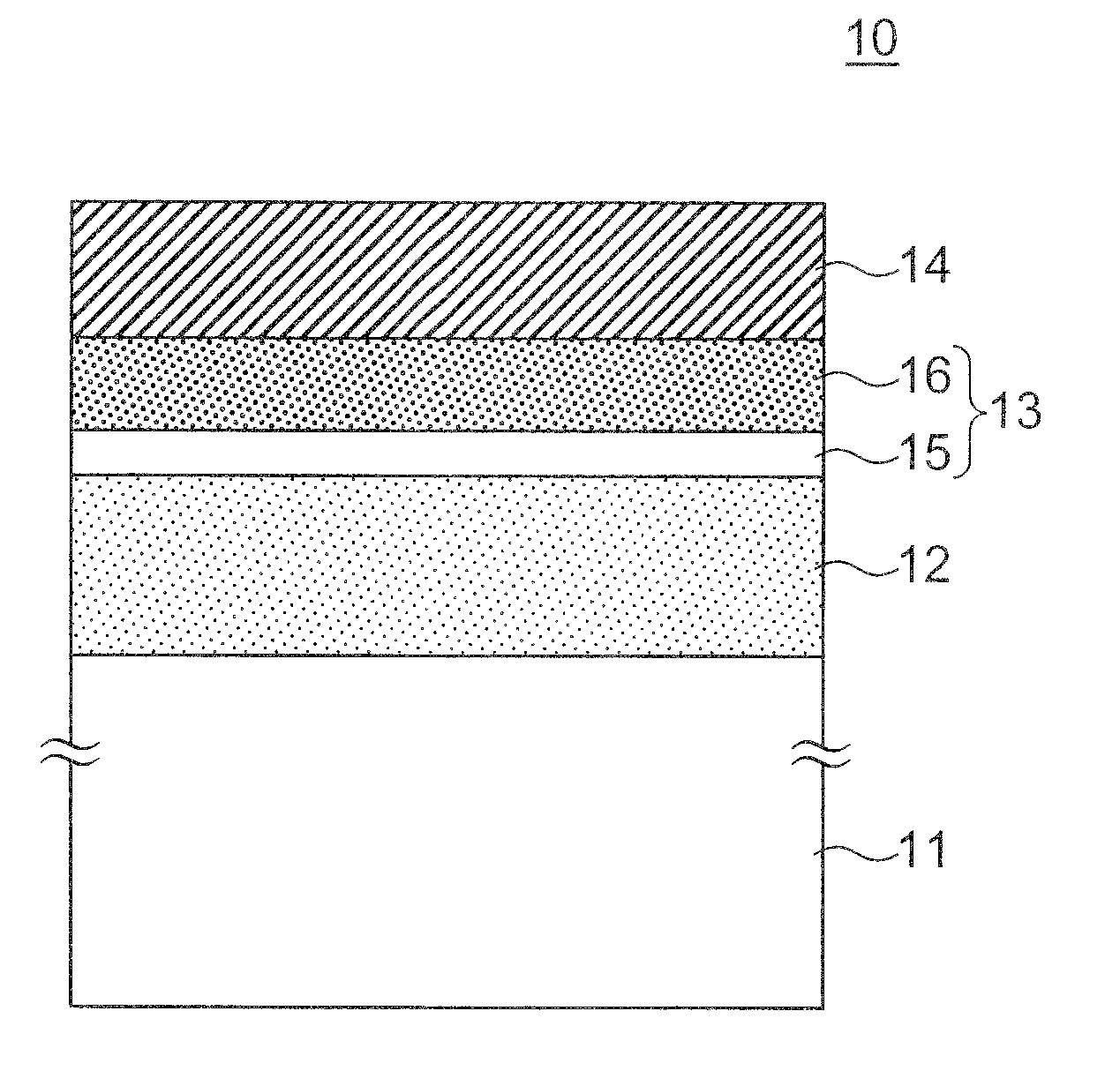
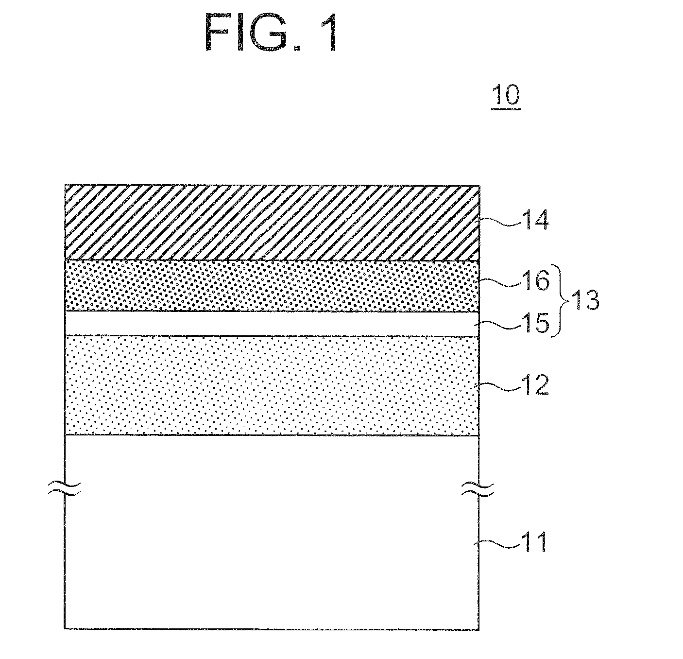
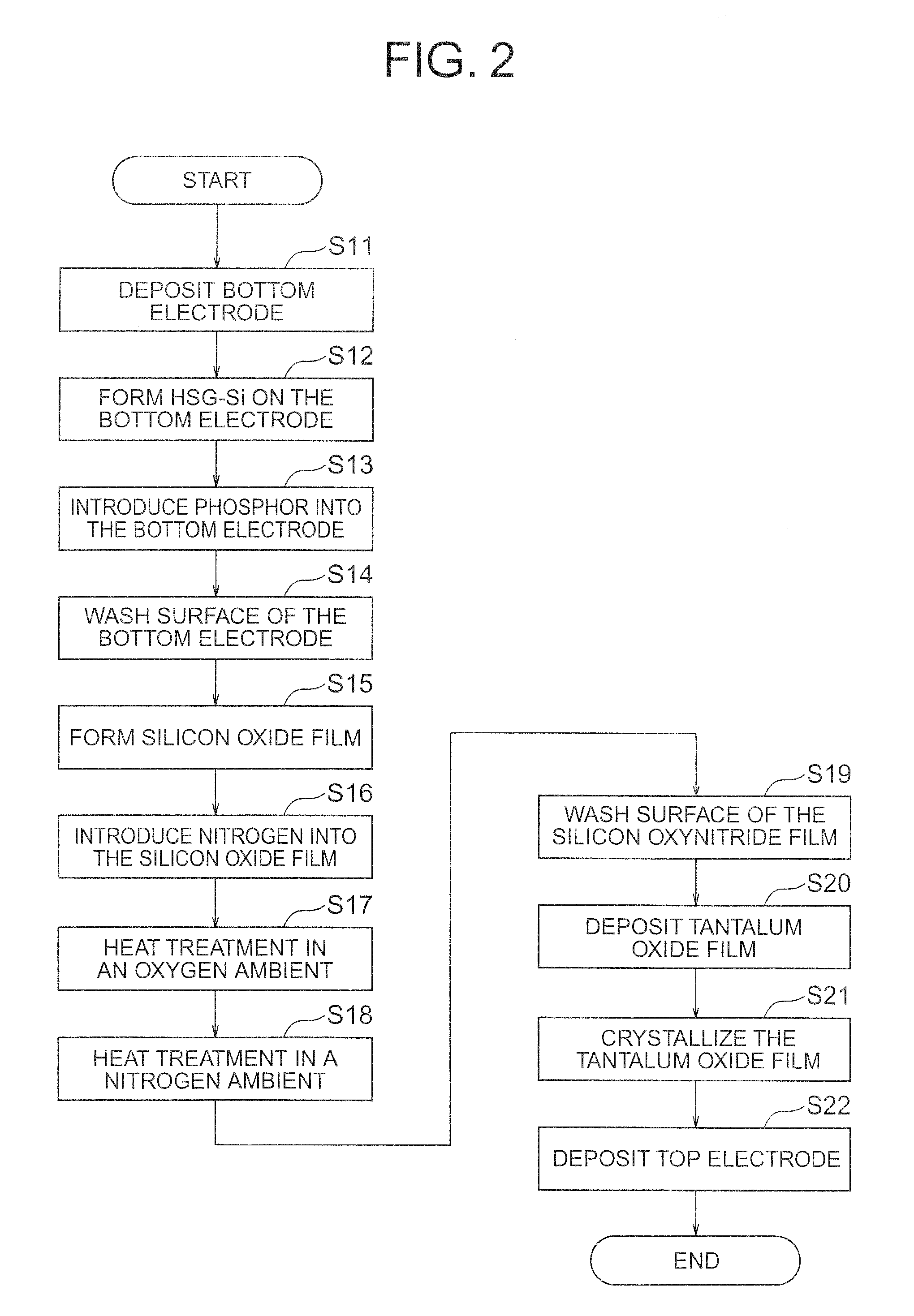
[0017] Now, an exemplary embodiment of the present invention will be described with reference to accompanying drawings. FIG. 1 schematically shows the structure of a capacitor in a semiconductor device manufactured by a method according to an embodiment of the present invention. The semiconductor device 10 is a configured as a DRAM device, for example, and includes an array of memory cells each including a MOSFET (not shown) formed in an underlying structure 11 and a capacitor depicted in the figure.

[0018] The capacitor includes a bottom electrode 12, a capacitor insulation film 13, and a top electrode 14. The bottom electrode 12 is configured by a polysilicon film heavily-doped with phosphor. The capacitor insulation film 13 has a two-layer structure including a 2-nm-thick silicon oxynitride (SiON) film 15 and an overlying 9-n-thick tantalum oxide (Ta2O5) film 16. Although not illustrated, the bottom electrode 12 has a hemispherical grained structure including a plurality of hemis...


PUM

PropertyMeasurementUnit
pressureaaaaaaaaaa
temperatureaaaaaaaaaa
areaaaaaaaaaaa

Abstract

A process for forming a capacitor in a semiconductor device includes the step of forming a two-layer capacitor insulation film including a silicon oxynitride film and a tantalum oxide film. The step for forming the silicon oxynitride film is performed at a first substrate temperature, and the step of forming the tantalum oxide film uses a heat treatment performed at a second substrate temperature. The second substrate temperature is lower than the maximum of the first substrate temperature, to provide a higher capacitance per unit area and a lower leakage current in the capacitor.

Description

[0001] This application is based upon and claims the benefit of priority from Japanese patent application No. 2006-282943, the disclosure of which is incorporated herein in its entirety by reference. BACKGROUND OF THE INVENTION [0002] (a) Field of the Invention [0003] The present invention relates to a method for manufacturing a semiconductor device and, more particularly, to a method for forming a stacked capacitor in a semiconductor device. [0004] (b) Description of the Related Art [0005] DRAM (dynamic random access memory) devices include an array of memory cells each for storing therein information. Each memory cell includes a MOSFET (metal-oxide-semiconductor field-effect-transistor) formed on a surface region of a silicon substrate and a storage capacitor or stacked capacitor overlying the MOSFET and connected thereto, and stores electric charge in the storage capacitor via the MOSFET. In recent years, the area occupied by each memory cell is drastically reduced along with dev...

Claims


Application Information

Patent Timeline
Patent Type & Authority Applications(United States)
IPC IPC(8): H01L21/283
CPCH01L28/40
Inventor KITAMURA, HIROYUKI
Owner ELPIDA MEMORY INC
Why Eureka
Try Eureka