Composition for forming porous film, porous film and method for forming the same, interlevel insulator film, and semiconductor device

a technology of porous film and insulator film, which is applied in the direction of crystalline aluminosilicate zeolites, semiconductor/solid-state device details, transportation and packaging, etc., can solve the problems of increasing the delay time of interconnection, hindering the enhancement of the performance of semiconductor circuits, and increasing the cost of siloxane polymer synthesis, etc., to achieve low dielectric constant, high film consistency, and mechanical strength sufficient

Inactive Publication Date: 2008-05-22
SHIN ETSU CHEM IND CO LTD +1
View PDF5 Cites 0 Cited by
  • Summary
  • Abstract
  • Description
  • Claims
  • Application Information

AI Technical Summary

Benefits of technology

[0026] The present invention has an object of providing a composition for film formation which can be formed into a porous film that excels in dielectric properties, adhesion, film consistency and mechanical strength, and that is easily thinned; and a porous film and a method for forming the same. The present invention has another object of providing a high-performing and highly reliable semiconductor device which contains the porous film inside.
[0028] Zeolite is a general term of crystalline porous alumino silicates. This crystal not only contains a number of pores having diameters of 0.4 to 0.8 nm or so, but also has an extremely high mechanical strength because of its crystal structure. It is known that the zeolite composed exclusively of silicon is hydrophobic, and its dielectric constant is estimated to be 1.5 to 1.7 or so according to a molecular orbital method. When zeolite micro-particles with such physical properties are added to the composition for coating film formation, the porous film is supplied with excellent mechanical properties and dielectric properties through heat treatment during film formation. These physical properties of zeolite are excellent as a material for a semiconductor porous film.
[0032] a coating step for coating this composition for forming a porous film; a subsequent drying step; and a heating step for zeolite structure growth. The present invention further provides a porous film prepared by using this composition for forming a porous film. This porous film can be applied to a semiconductor fabrication process and excels in dielectric properties and mechanical strength.
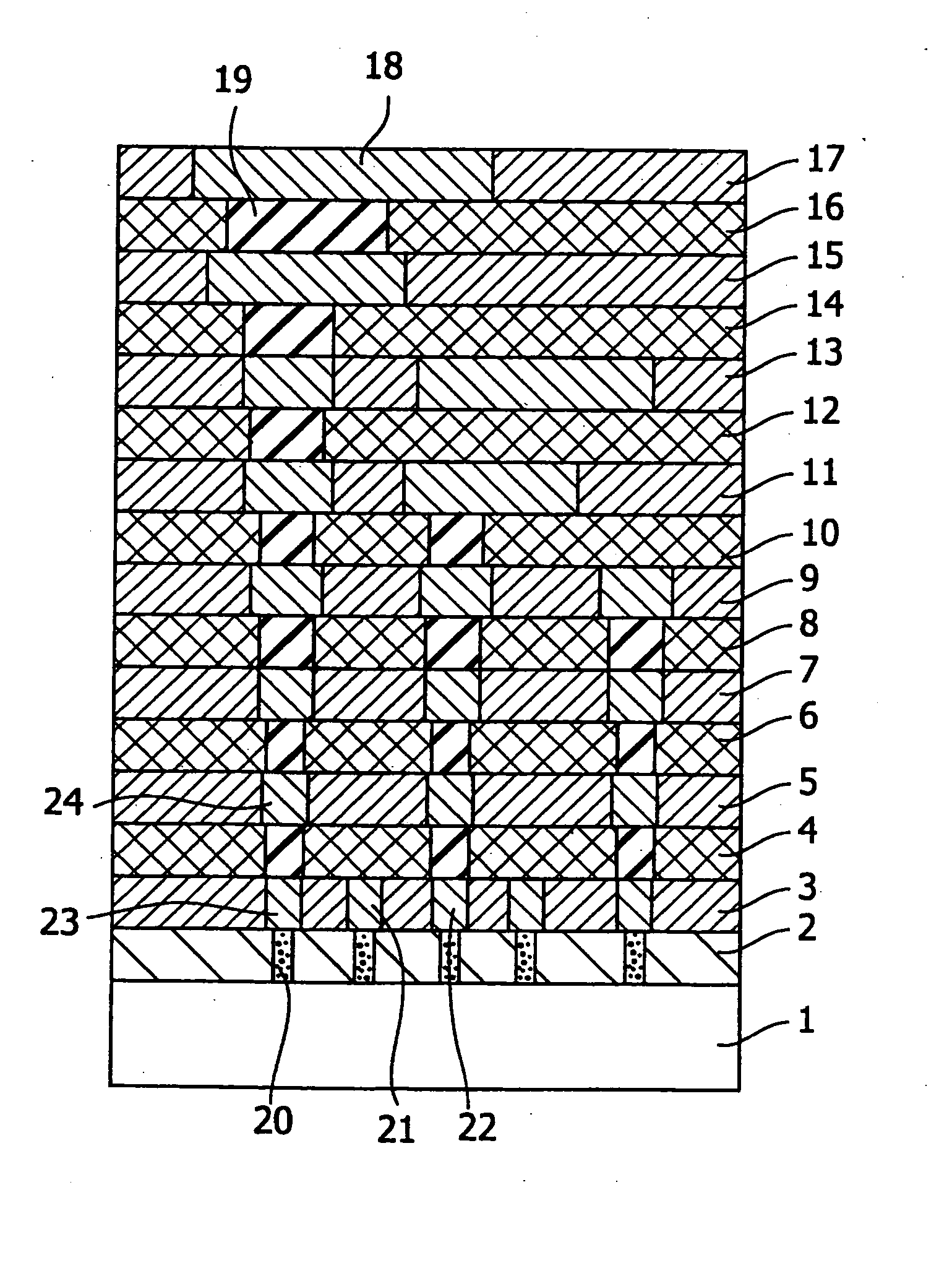
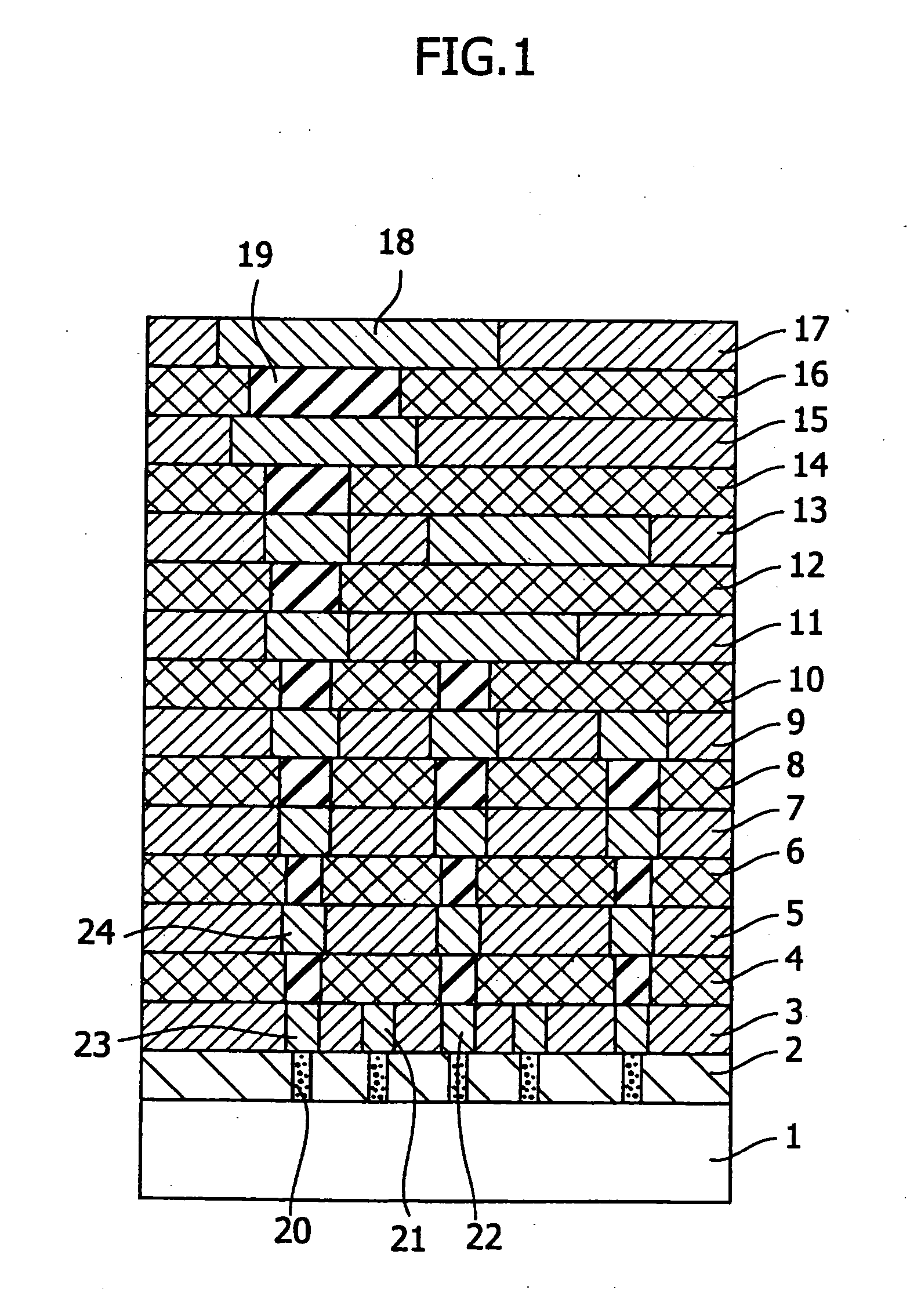
[0036] This realizes a semiconductor device which contains a porous film having high film consistency, a low dielectric constant, and mechanical strength sufficient for the fabrication of semiconductor devices as an insulator film of the multilayered interconnections. The proper control of the thickness of the porous film facilitates the fabrication of the semiconductor. Since the zeolite-containing film is an insulator film with a low dielectric constant, the parasitic capacitance around the multilayered interconnections is reduced, thereby achieving high-speed and low-power operations of the semiconductor device.
[0037] In the semiconductor device of the present invention, the porous film may be preferably present in an insulator film between metal interconnections in the same layer of the multilayered interconnections or in the interlevel insulator film between the vertically stacked metal interconnection layers. This arrangement can achieve a high-performing and highly reliable semiconductor device.
[0038] The use of the composition for forming a porous film of the present invention facilitates the formation of a porous film having a properly controlled thickness. This porous film has a low dielectric constant, and excels in adhesion, film consistency, and mechanical strength. In addition, the use of the porous film made from the composition of the present invention as the insulator film of the multilayered interconnections can achieve a high-performing and highly reliable semiconductor device.

Problems solved by technology

In the fabrication of semiconductor integrated circuits, as the circuits are packed tighter, an increase in interconnection capacitance, which is a parasitic capacitance between metal interconnections, leads to an increase in interconnection delay time, thereby hindering the enhancement of the performance of semiconductor circuits.
However, use of this structure alone has limits in the enhancement of the performance, so the reduction in interconnection capacitance is an urgent necessity for higher performance of semiconductors.
However, these methods have respective major drawbacks as follows.
In the first method for forming a porous film, the synthesis of the precursor solution of the siloxane polymer increases the cost.
In addition, the formation of the coating film by coating the precursor solution increases the amount of silanol groups remaining in the coating film, which causes a degassing phenomenon indicating the evaporation of water and the like in the heat treatment process that is conducted later and which also deteriorates the film quality due to the porous film absorbing humidity.
In the second method for forming a porous film, the speed control of the evaporation of the solvent from the wet gel requires a special type of coating device, which increases the cost.
In addition, a significant amount of silanol remains on the surface of the micro-pores which must be silanized because otherwise hygroscopicity is high and the film quality decreases.
The silanization makes the process more complicated.
In the case where a wet gel is formed by the CVD process, it is necessary to use a special type of CVD device which is different from the plasma CVD device generally used in the semiconductor process, thereby also increasing the cost.
This makes it difficult to set the relative permittivity of the porous film to 2 or below.
However, it is not preferable because it makes the manufacturing process complicated and increases the cost.
However, these methods have problems as follows.
In the first method, the powdered porous member can be easily formed, but it is impossible to form a porous film as a thin film on the substrate which is used for the fabrication of semiconductor devices.
In the second method, a porous member can be formed into a thin film, but it is impossible to control the orientation of micro-pores, and it is also impossible to form a uniform thin film in a wide area.
However, in this method, too, the restriction of the solute concentration makes it difficult to properly control the thickness of a coating film, thereby making it difficult to apply it to a practical semiconductor fabrication process.
When this solution is diluted with water, the thickness of the coating film becomes controllable, but the speed of polycondensation of the silica component increases to lose stability of the coating solution.
However, these methods form a zeolite film in a sealed container such as an autoclave, and are not practically used in a fabrication process for semiconductor devices.
Because it is considered that a coefficient of elasticity must be 5 GPa or higher for use in an actual semiconductor fabrication process, these inventions cannot be said to be satisfactory for mechanical strength.
As described hereinbefore, the conventional porous films have problems wherein the film consistency is low and the thickness is not properly controllable, and as a result, it is difficult even to prepare a coating solution from the material using zeolite.
Therefore, when a conventional porous film is integrated into multilayered interconnections of a semiconductor device as an insulator film, the porous film is difficult to be thinned, the film consistency is low, and the film thickness is not properly controllable.
These problems decrease the yield of the semiconductor device fabrication or make the fabrication itself difficult.
Furthermore, a porous film with a low mechanical strength deteriorates the reliability of the semiconductor device, even if it can be used for semiconductor fabrication.

Method used


Image

  • Composition for forming porous film, porous film and method for forming the same, interlevel insulator film, and semiconductor device
  • Composition for forming porous film, porous film and method for forming the same, interlevel insulator film, and semiconductor device

Examples


preparation example 1

[0074] A mixture of 14.6 g of tetraethoxysilane and 25.4 g of 1 mol / L of aqueous solution of tetrapropylammonium hydroxide was stirred for 3 days at room temperature. Then, the reaction mixture was stirred for 3 days at 80° C. to obtain a zeolite sol having an average particle diameter of 75 nm.

[0075] Next, 8 g of aqueous solution of 28 wt % ammonia, 512 g of ultra pure water, 960 g of ethanol, and the aforementioned zeolite sol were mixed at room temperature. Then, 32 g of tetraethoxy silane and 24 g of methyl trimethoxy silane were added to the mixture and stirred for 4 hours at 65° C. Then, 320 g of propylene glycol monopropyl ether was added to the obtained reaction solution and concentrated until the weight of the solution reached 320 g to obtain a composition solution for coating.

Determination of the Zeolite Structure

[0076] After having been powdered by vacuum drying, the zeolite sol was studied by using an X-ray diffraction device: M18XHF-SRA (from MAC Science co., Ltd.)....

preparation example 2

[0078] Another composition solution for coating was prepared in the same manner as in Preparation Example 1 except that 32.4 g of 1 mol / L of aqueous solution of tetrabutylammonium hydroxide was used instead of 25.4 g of 1 mol / L of aqueous solution of tetrapropylammonium hydroxide.

preparation example 3

[0079] Another composition solution for coating was prepared in the same manner as in Preparation Example 1 except that 32 g of tetramethoxysilane was used instead of 32 g of tetraethoxysilane.


PUM

PropertyMeasurementUnit
particle diameteraaaaaaaaaa
relative permittivityaaaaaaaaaa

Abstract

The present invention provides a composition for film formation which can form a porous film that excels in dielectric properties, adhesion, film consistency and mechanical strength, and that is easily thinned; a porous film and a method for forming the same, and a high-performing and highly reliable semiconductor device which contains the porous film inside. More specifically, the composition for forming a porous film comprises a solution containing an amorphous polymer which is obtained by hydrolyzing and condensing at least one silane compound expressed by the general formula (R1)nSi(OR2)4-n, and a zeolite sol which is formed by using a quaternary ammonium hydroxide. The method for forming a porous film comprises a coating step for coating the composition for forming a porous film; a subsequent drying step; and a porousness forming step.

Description

RELATED APPLICATIONS [0001] This application is a continuation application of U.S. application Ser. No. 10 / 703,374 filed on Nov. 7, 2003, which claims priority from Japanese Patent Application No. 2002-3239128 filed on Nov. 13, 2002, the disclosures of which are incorporated by reference herein in their entirety.BACKGROUND OF THE INVENTION [0002] 1. Field of the Invention [0003] The present invention relates to a composition for film formation which can be formed into a porous film that excels in dielectric properties, adhesion, film consistency and mechanical strength, and has reduced absorption; a porous film and a method for forming the same; and a semiconductor device which contains the porous film inside. [0004] 2. Description of the Related Art [0005] In the fabrication of semiconductor integrated circuits, as the circuits are packed tighter, an increase in interconnection capacitance, which is a parasitic capacitance between metal interconnections, leads to an increase in int...

Claims


Application Information

Patent Timeline
Patent Type & Authority Applications(United States)
IPC IPC(8): B32B5/18B05D5/00C08J9/22C01B39/04B32B25/20C09D183/04H01L21/312H01L21/316H01L21/768H01L23/522H01L23/532
CPCC08K3/34C08L83/02C09D183/04H01L23/5222H01L23/53228H01L2924/0002H01L23/5329H01L2924/12044H01L2924/00Y10T428/249953Y10T428/31663
Inventor OGIHARA, TSUTOMUYAGIHASHI, FUJIONAKAGAWA, HIDEOSASAGO, MASARU
Owner SHIN ETSU CHEM IND CO LTD
Why Eureka
Try Eureka