

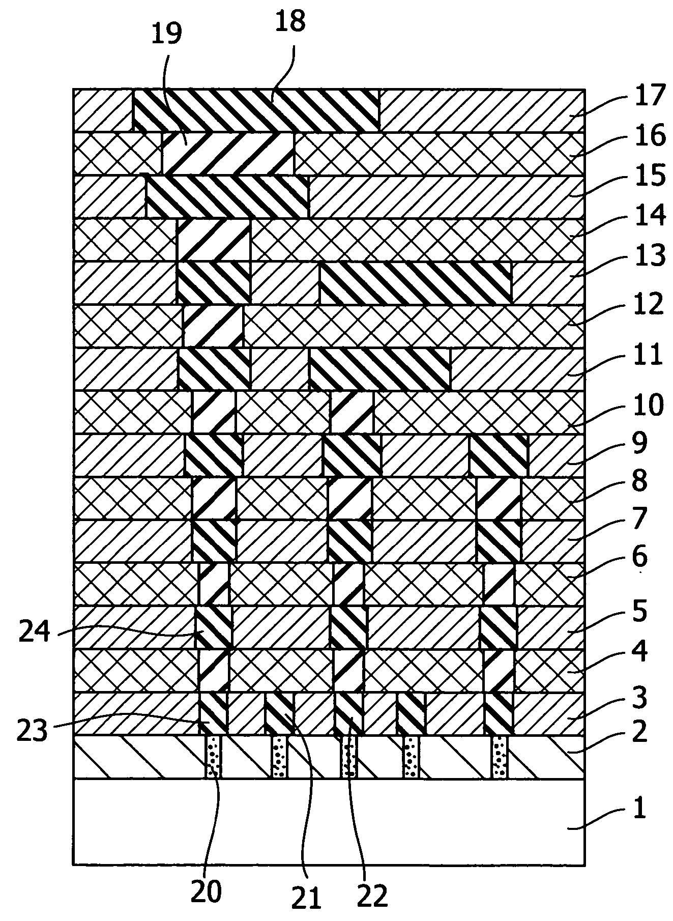
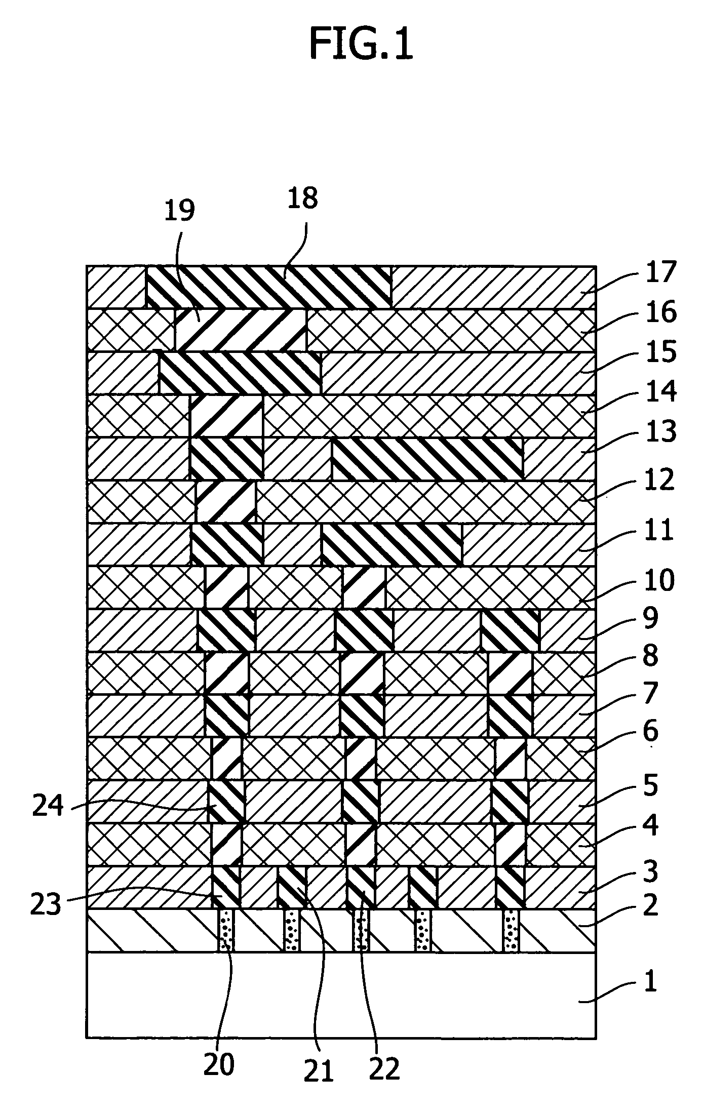
Composition for forming porous film, porous film and method for forming the same, interlevel insulator film
a technology of porous film and interlayer, which is applied in the direction of bulk negative resistance effect devices, coatings, and silicon oxides, can solve the problems of increasing interconnection delay time, increasing the cost of synthesis of the precursor solution of the siloxane polymer, and hindering the enhancement of the performance of semiconductor circuits. , to achieve the effect of reducing the parasitic capacitance of the area around the multi-level interconnect, reducing the hygroscopic property of the porous film
- Summary
- Abstract
- Description
- Claims
- Application Information
AI Technical Summary
Benefits of technology
Problems solved by technology
Method used
Image

Examples
examples 1 – 6
EXAMPLES 1–6
[0073]The mixture of 30.4 g tetramethoxysilane and 8.0 g water was stirred at room temperature, while 0.2 ml hydrochloric acid was added thereto all at once. After stirred for a few minutes, the reacting solution generated heat and became a uniform solution. It was stirred 1 hour further at room temperature, producing a slightly viscous solution. According to the analysis with a gel permeation chromatography using tetrahydrofuran as a moving bed, the siloxane produced had weight-average molecular weight of 1,250 and number average molecular weight of 822 based on polystylene. The 6.82 g trimethyloctadecylammonium chloride was added to this solution and stirred to produce a uniform solution. Then an additional one hour of agitation produced a transparent and colorless solution.
[0074]This was used as a stock solution. The composition for forming porous film was obtained by diluting the stock solution with a prescribed quantity of solvent as shown in Table 1, wherein DMF is...
examples 7 – 13
EXAMPLES 7–13
[0078]The mixture of 15.2 g tetramethoxysilane, 13.6 g methyltrimethoxysilane and 7.0 g water was stirred, while 0.2 ml of 1N hydrochloric acid solution was added all at once thereto. After stirred for a few minute, the reacting solution generated heat and became a uniform solution. It was stirred 1 hour further at room temperature, and the resulting solution was analyzed with a gel permeation chromatography. It had weight-average molecular weight of 1,872 and number average molecular weight of 839 based on polystylene. The 6.4 g trimethylhexadecylammonium chloride was added to this solution and stirred further for one hour produced a transparent and colorless solution.
[0079]This was used as a stock solution. The composition for forming porous film was obtained by diluting the stock solution with a prescribed quantity of solvent as shown in Table 2.
example 1
COATING EXAMPLE 1
[0083]The solution in Example 1 was applied on an 8 inch wafer with a spin coater at 2,000 rpm for 1 minute to produce a film on the wafer. The film was heated on a hot plate at 100° C. for 1 minute. Then, the film had thickness of 12,600 Å. After the film was further heated at 150° C. for 1 minute, it was heated at 400° C. for 1 hour in a nitrogen atmosphere in a clean oven. The obtained film had thickness of 10,200 Å. The dielectric constant of the coated film had 1.8 in a CV method using an automatic mercury probe. Moreover, it had specific surface area of 3,100 m2 / g according to the method of gas adsorption. A central value of the pore diameters was 2.0nm and it was confirmed that the pores having pore size of more than 3.0 nm did not substantially existed. The film had modulus of 8.5 GPa according to the measurement of a Nanoindenter.
PUM
| Property | Measurement | Unit |
|---|---|---|
| dielectric constant | aaaaa | aaaaa |
| relative permittivity | aaaaa | aaaaa |
| relative permittivity | aaaaa | aaaaa |
Abstract
Description
Claims
Application Information